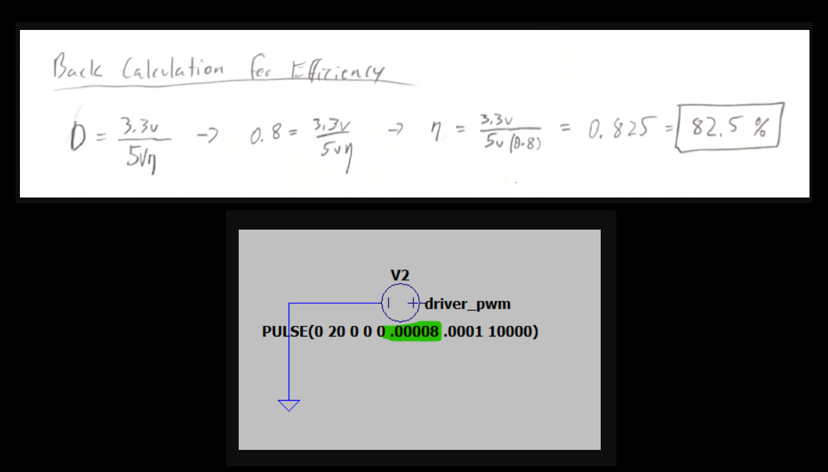
Computational Estimation of Magnetic Flux Density for Layered Annular Sector Coils
Building on my first attempt using circular loops, this post details a more refined Python analysis of airgap flux density. This version increases realism by modeling windings as multi-layer annular sectors – a shape better reflecting my design – calculated using the Biot-Savart law. For windings supported by materials like FR4 PCB (µᵣ ≈ 1, similar to air), the Biot-Savart ‘air’ calculation holds well. Consequently, these results should be reasonably close to FEA simulations configured to neglect secondary effects. Finite Element Analysis (FEA) is still the logical progression and my planned next step in evaluating this design.
(The Python notebook can be downloaded at the bottom of the page)
Motivation: Towards Realistic Coil Geometry
A real motor winding isn’t just a single loop. It consists of multiple turns wound layer upon layer. To capture this more accurately, this simulation models each layer as a series of contracting annular sectors. Imagine starting with the outermost boundary of the coil cross-section and then winding inwards, turn by turn, with a defined spacing. Furthermore, multiple such layers are stacked axially, offset slightly from each other. This approach provides a much better geometric approximation of the actual current distribution compared to a single, simple loop.
The Approach: Iterative Geometry and Grid-Based Biot-Savart
-
Generating the Winding Paths:
-
The core shape is an annular sector (a slice of a doughnut).
-
The create_single_sector_perimeter_angled_closed function generates the points defining the perimeter of one such sector.
-
The key generate_disconnected_loops function takes the initial outer/inner radii and angle and iteratively calculates the geometry for subsequent turns within a layer. It reduces the outer radius and increases the inner radius by the SPIRAL_SPACING for each “turn,” also adjusting the angular width slightly to approximate constant wire width. This continues until the inner and outer radii meet or a maximum loop count (MAX_LOOPS_PER_LAYER) is reached.
-
This process creates a list of 2D loop paths representing the turns within a single layer.
-
Multiple layers are then created by copying this 2D loop list and assigning different Z-coordinates based on NUM_LAYERS and LAYER_OFFSET.
-
-
Defining the Calculation Space:
-
Instead of calculating the field everywhere (computationally expensive), we define a specific region of interest: the airgap.
-
The annulus_grid_points_xyz_angle function generates a grid of points within an annular sector located at the specified AIRGAP_DISTANCE from the first layer. The density of this grid is controlled by NUM_RADIAL_GRID and NUM_ANGULAR_GRID.
-
-
Applying Biot-Savart:
-
The standard biot_savart_segment_at_point function remains the workhorse. It calculates the infinitesimal magnetic field vector (dB) produced by a short, straight segment of current-carrying wire (dl_vec) at a specific point in space (point).
-
The main calculation loop iterates through every point in the airgap grid.
-
For each airgap point, it then iterates through every segment of every loop in every layer.
-
It calls biot_savart_segment_at_point for each segment and sums up all the resulting dB vectors to get the total magnetic field vector B = (Bx, By, Bz) at that specific airgap grid point.
-
Visualization and Results:

The script generates three key visualizations:
-
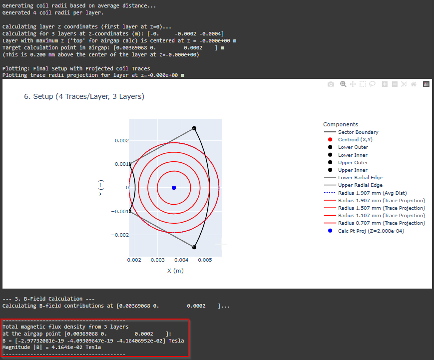
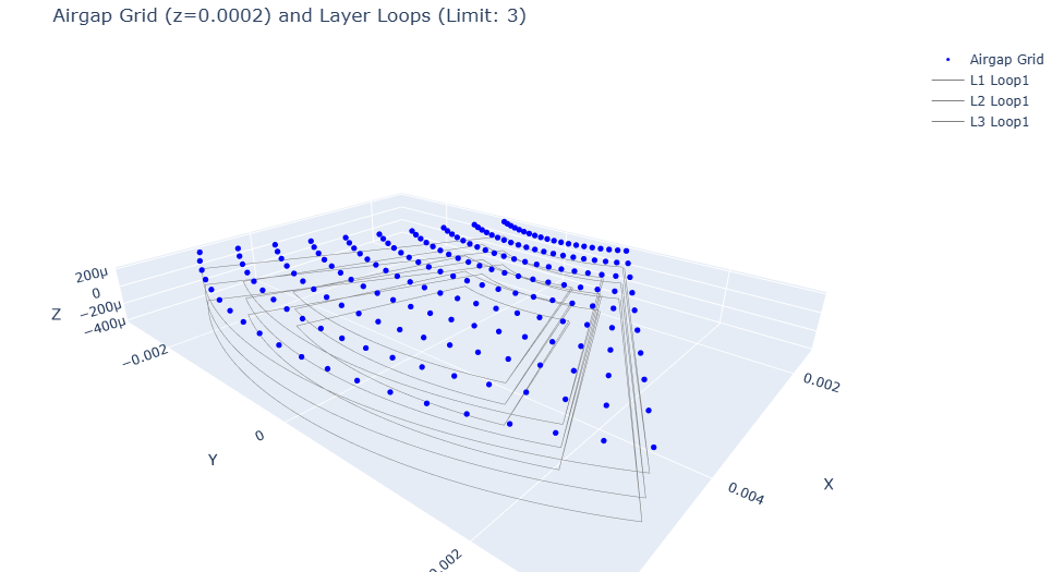
3D Grid & Paths: Shows the physical layout of the multi-layer coil loops (grey lines) and the grid points in the airgap (blue dots) where the field is calculated. This helps verify the geometry setup.
-
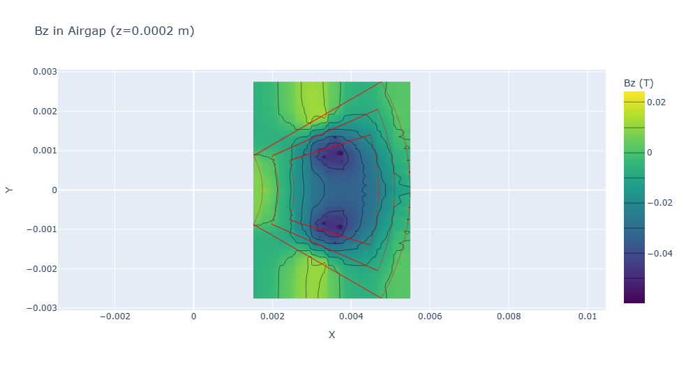
Bz Heatmap: Displays the calculated Z-component of the magnetic field (Bz) as a 2D heatmap on the airgap plane. The outlines of the 2D loops are overlaid in red for context. This is often the most critical component for axial flux machine performance.
-
B-Field Magnitude Markers: A 3D plot showing the coil loops again, but this time with markers at the airgap grid points. The color of each marker represents the magnitude (|B|) of the magnetic field at that point. (Initially, go.Cone glyphs were used to show direction, but rendering issues with Plotly v6.0.1 when combining many cones and lines necessitated this switch to markers for reliability).
Limitations of the Analytical Approach
While more refined, this model still relies on assumptions and has limitations:
-
Idealized Geometry: Assumes perfect annular sectors and uniform current density within wires.
-
No Eddy Currents: Doesn’t account for induced currents in conductive materials.
-
Computational Cost: Calculating the field from every segment for every grid point can become slow, especially with high point densities or many layers/turns.
Next Steps: Embracing FEA
These limitations highlight why Finite Element Analysis (FEA) is the standard tool for detailed motor design. FEA can:
-
Model complex 3D geometries accurately.
-
Incorporate non-linear material properties like B-H curves and saturation.
-
Calculate eddy currents and other secondary effects.
My next step in this learning journey will be to explore open-source FEA tools (like FEMM for 2D) to model this same axial flux motor configuration and compare the results.
Conclusion and Comparison:
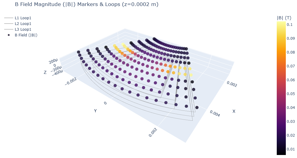
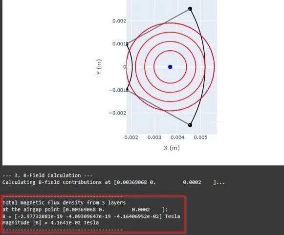
Comparison of magnetic flux density calculations reveals good agreement between the simplified circular estimation and the detailed spatial analysis near the geometric centroid, both yielding approximately 0.04 T. However, the detailed analysis highlights significant spatial variation missed by the simpler model, with flux density increasing to nearly 0.1 T towards the radial edges. The next step will involve Finite Element Analysis (FEA) to provide a more comprehensive simulation and further validate these analytical findings.
(Full Python Notebook will be added in the next 2 days)