Author: gknow81

  • September 2024 – Trees & Cleaning

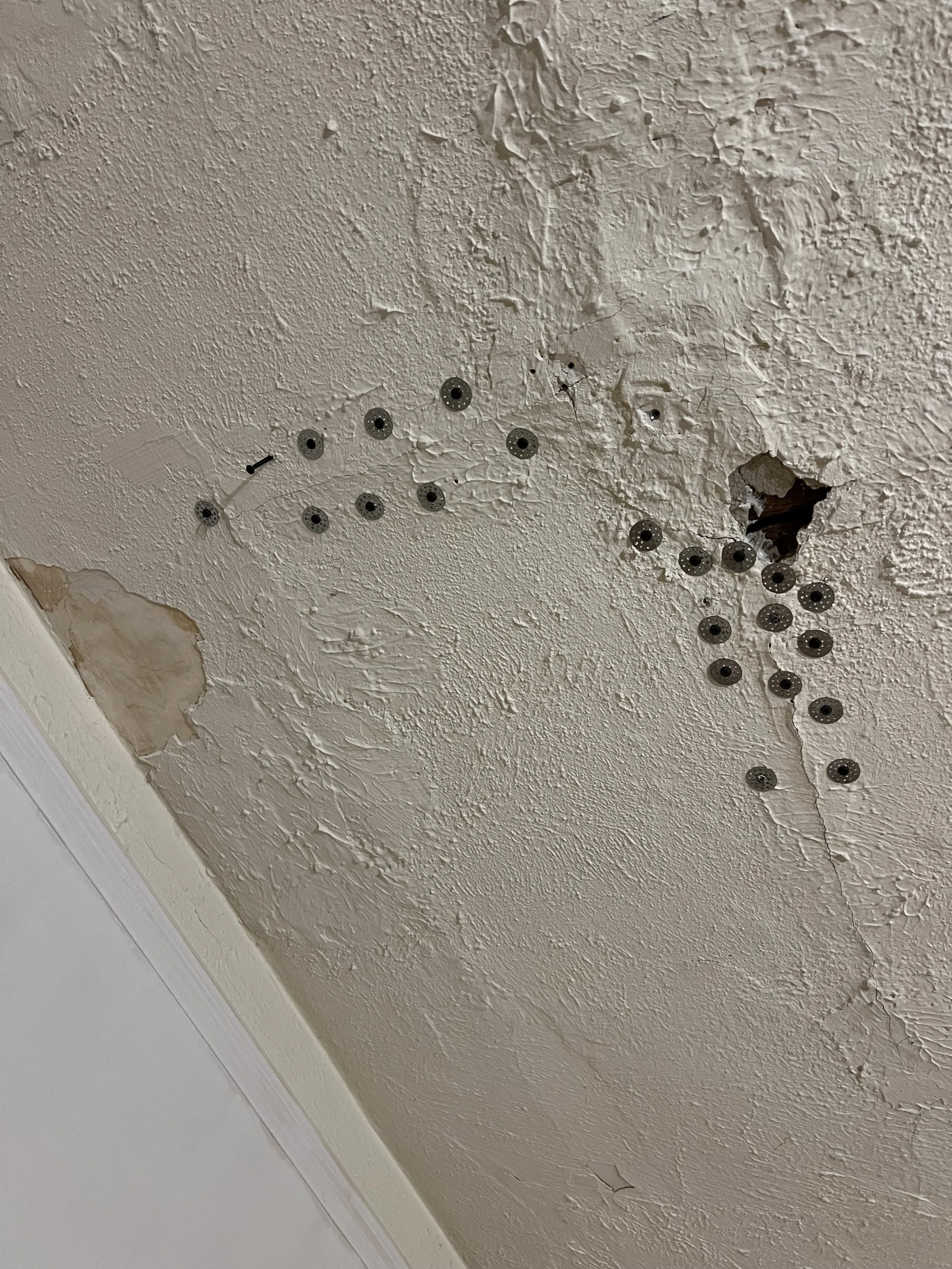
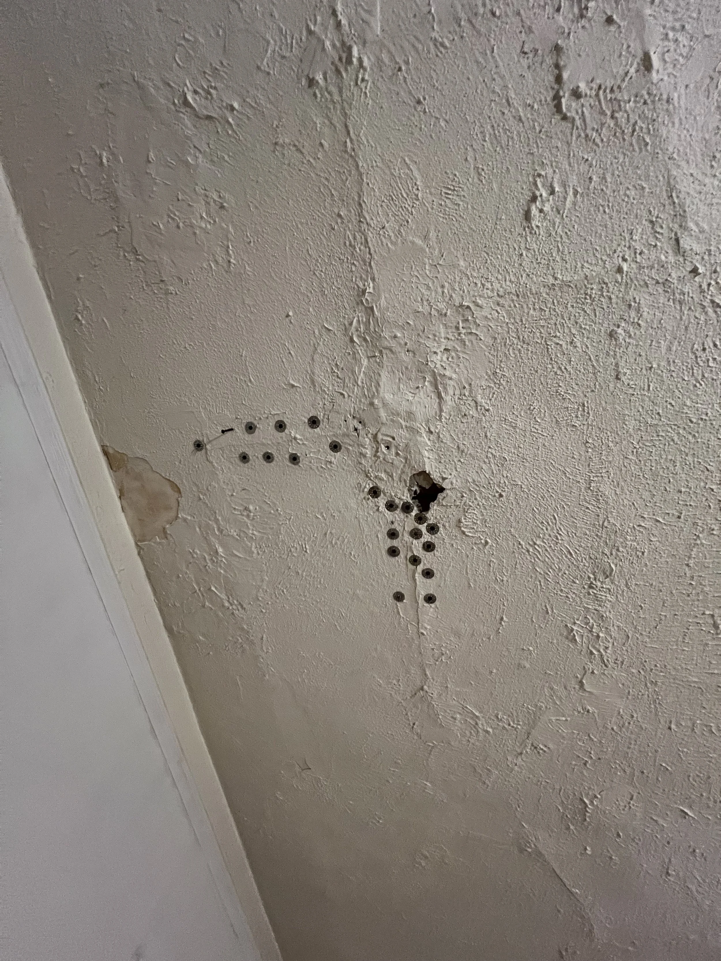
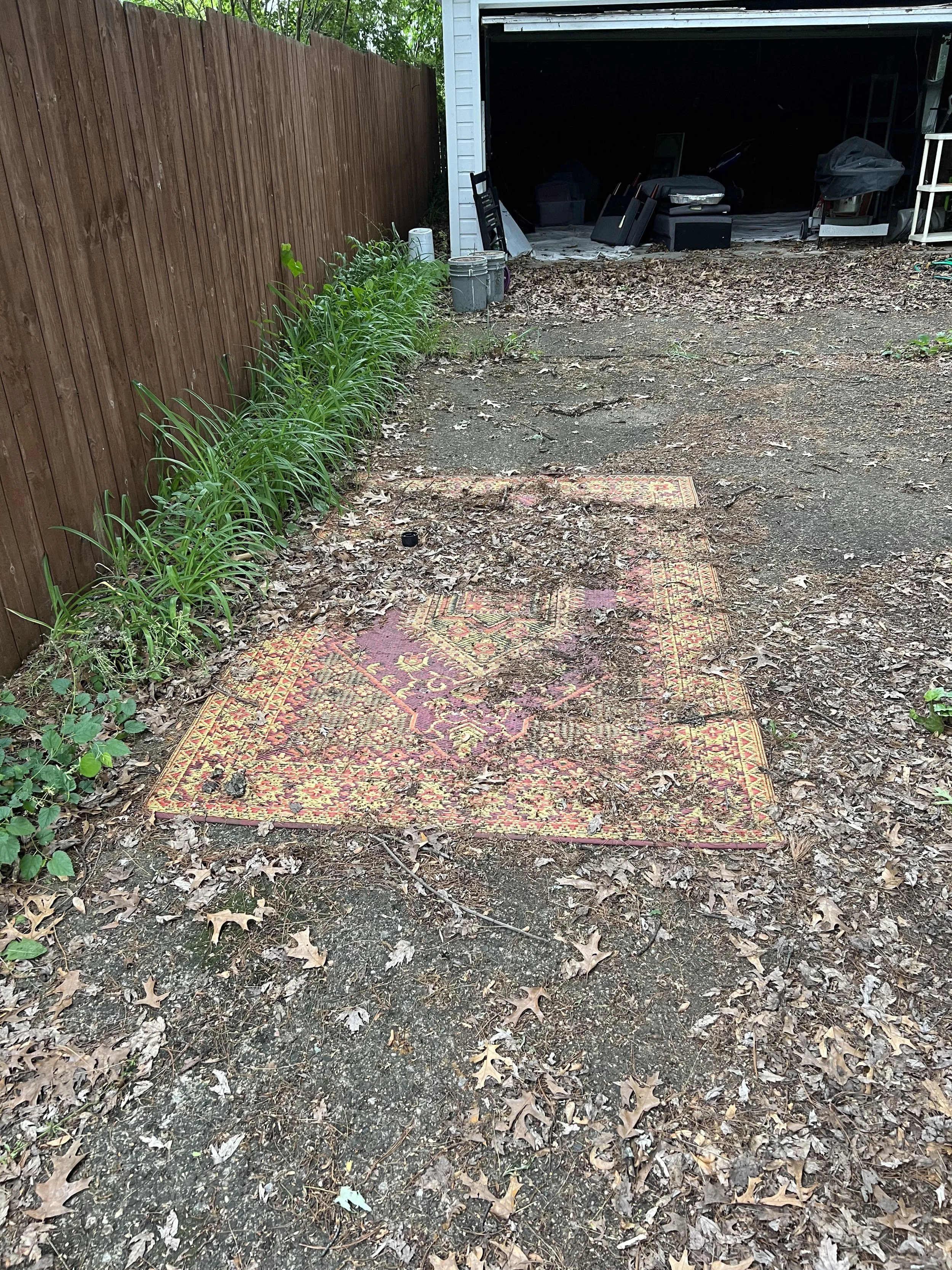
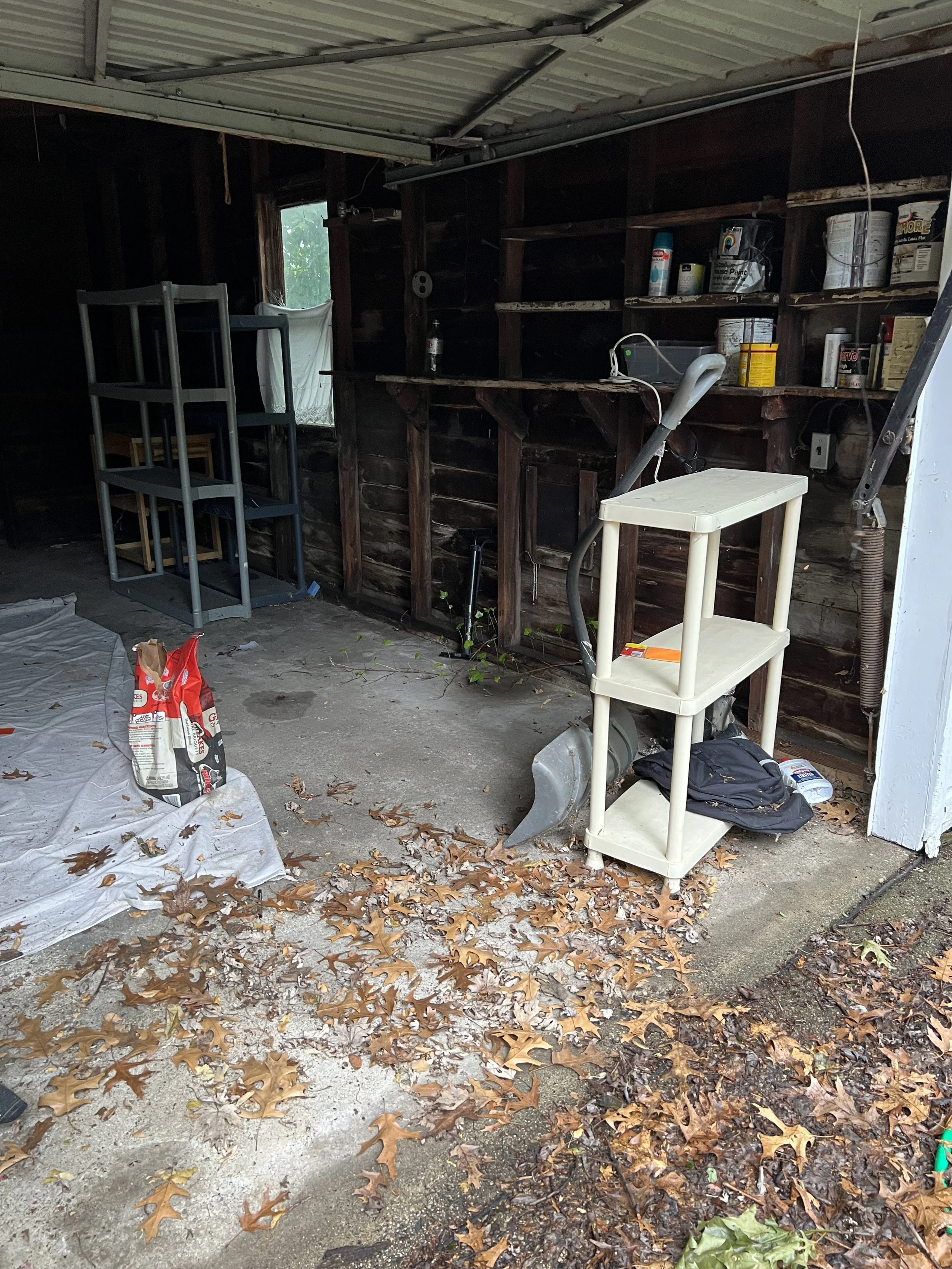
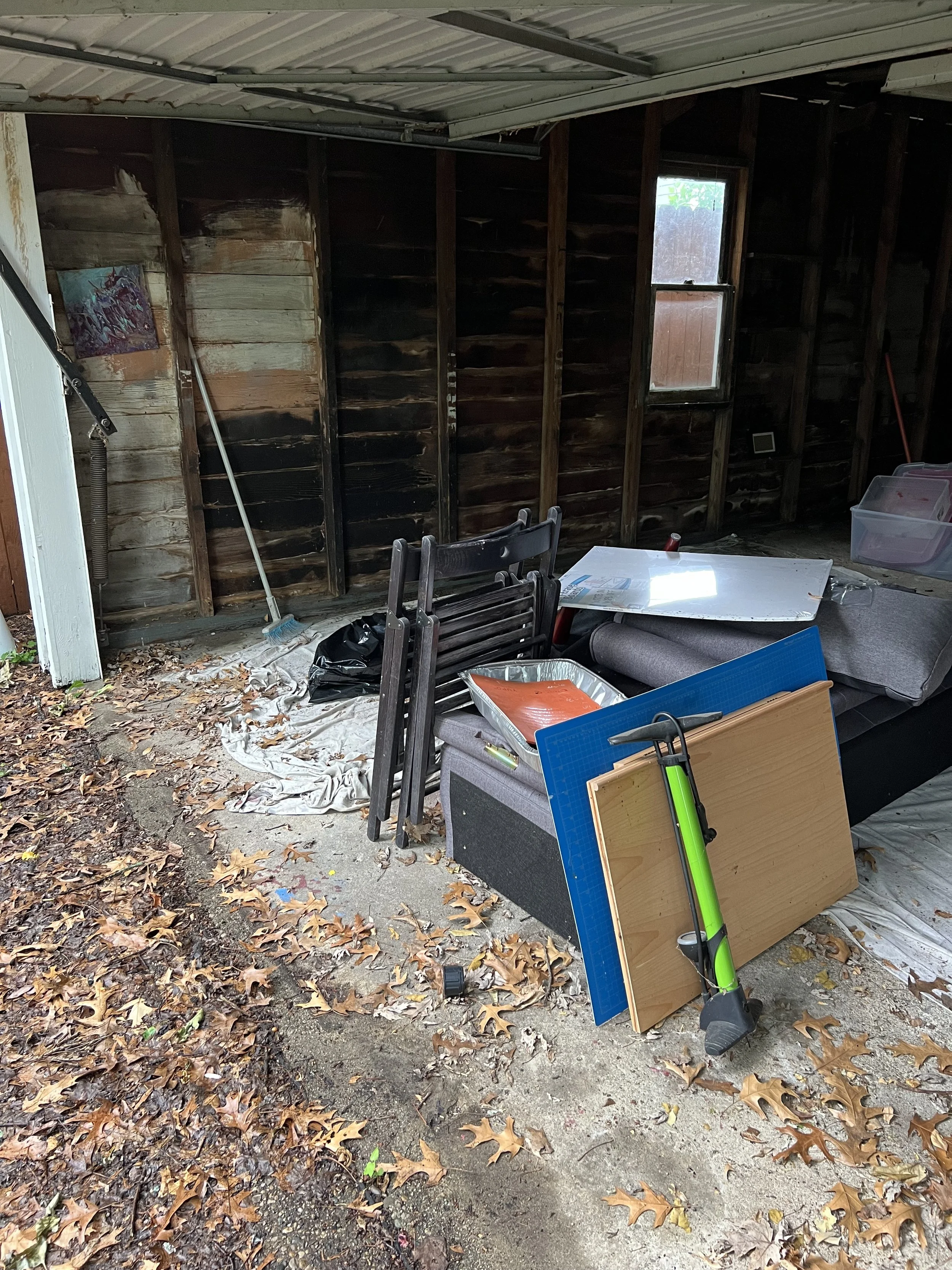
    Continuing with the theme of not documenting much, I have little to show from this month in the form of pictures.

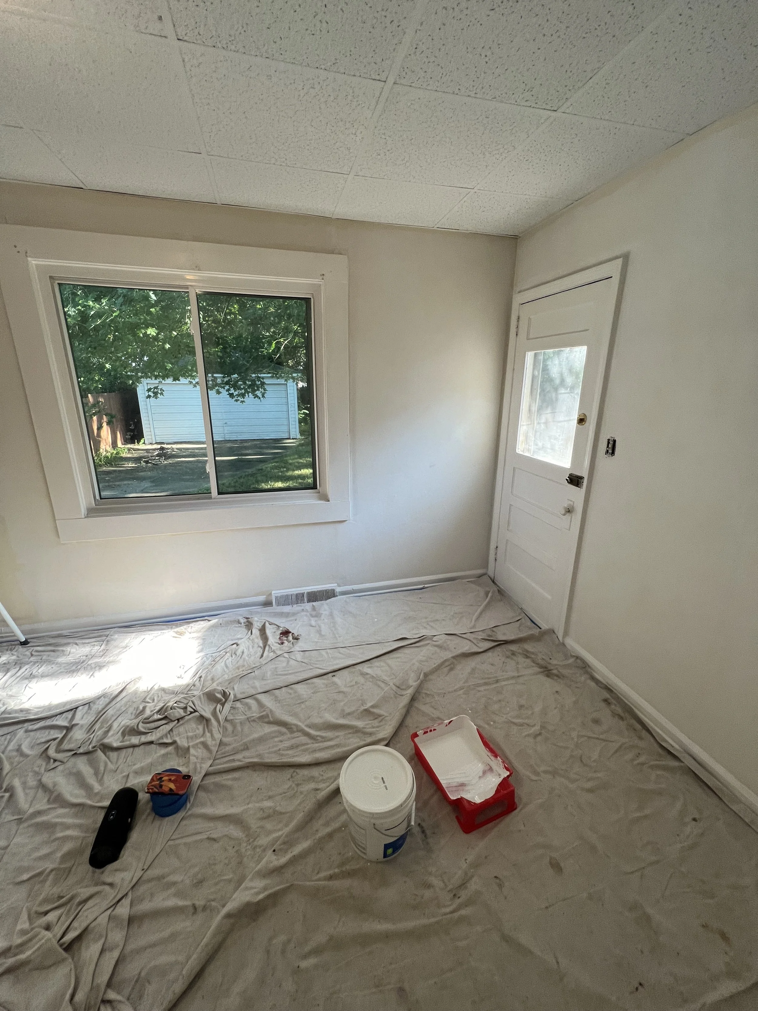
    September continued with painting, part 1 of repairing the defrost component in my fridge, cosmetic repairs, and the start of tree removal.

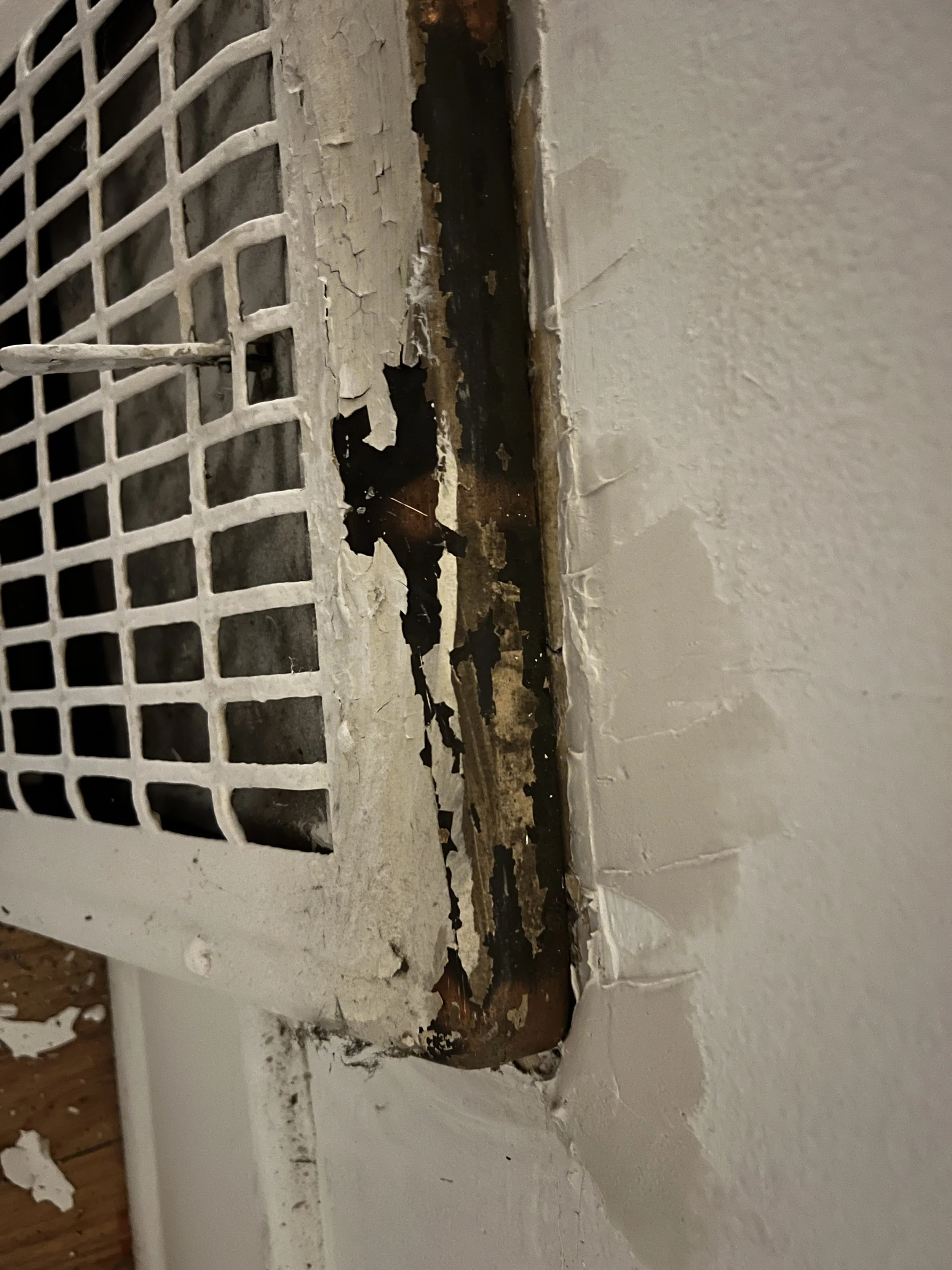
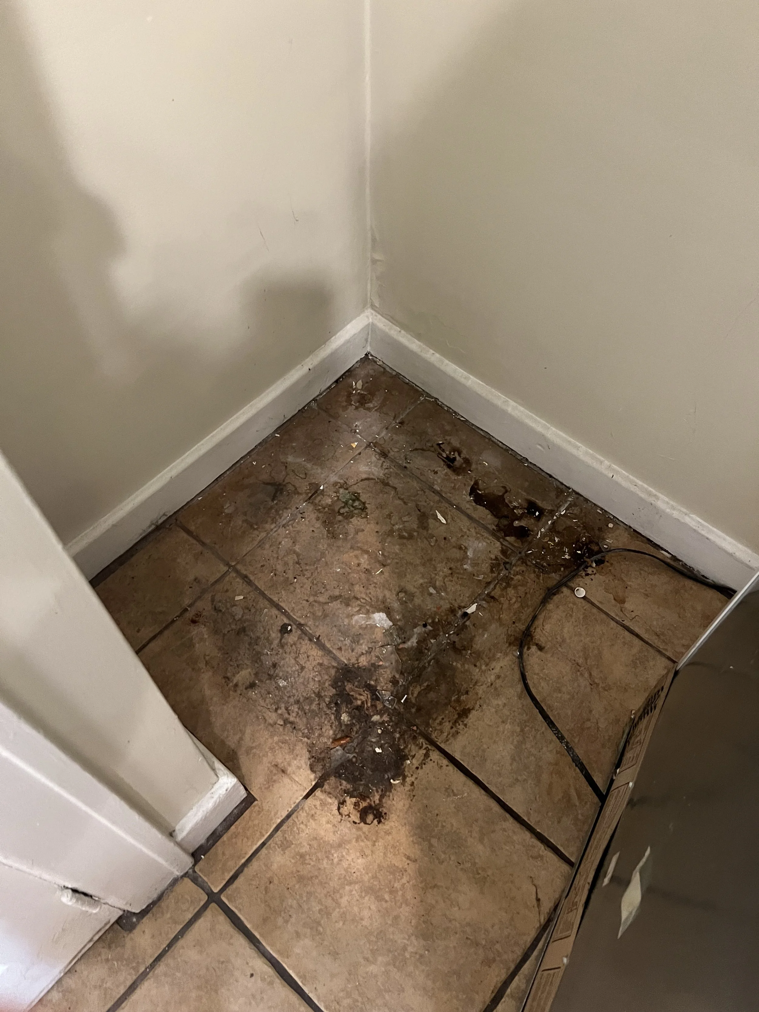
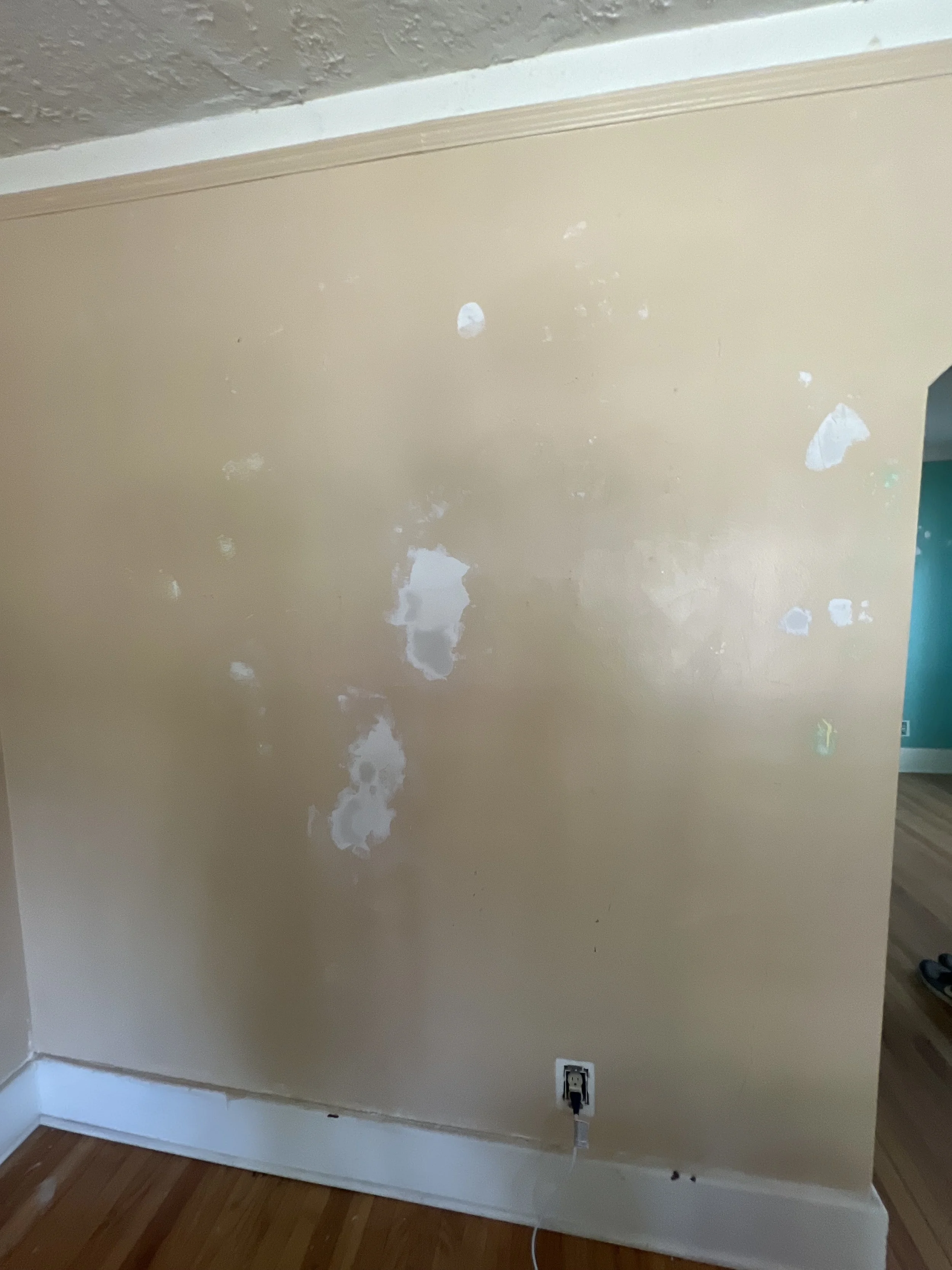
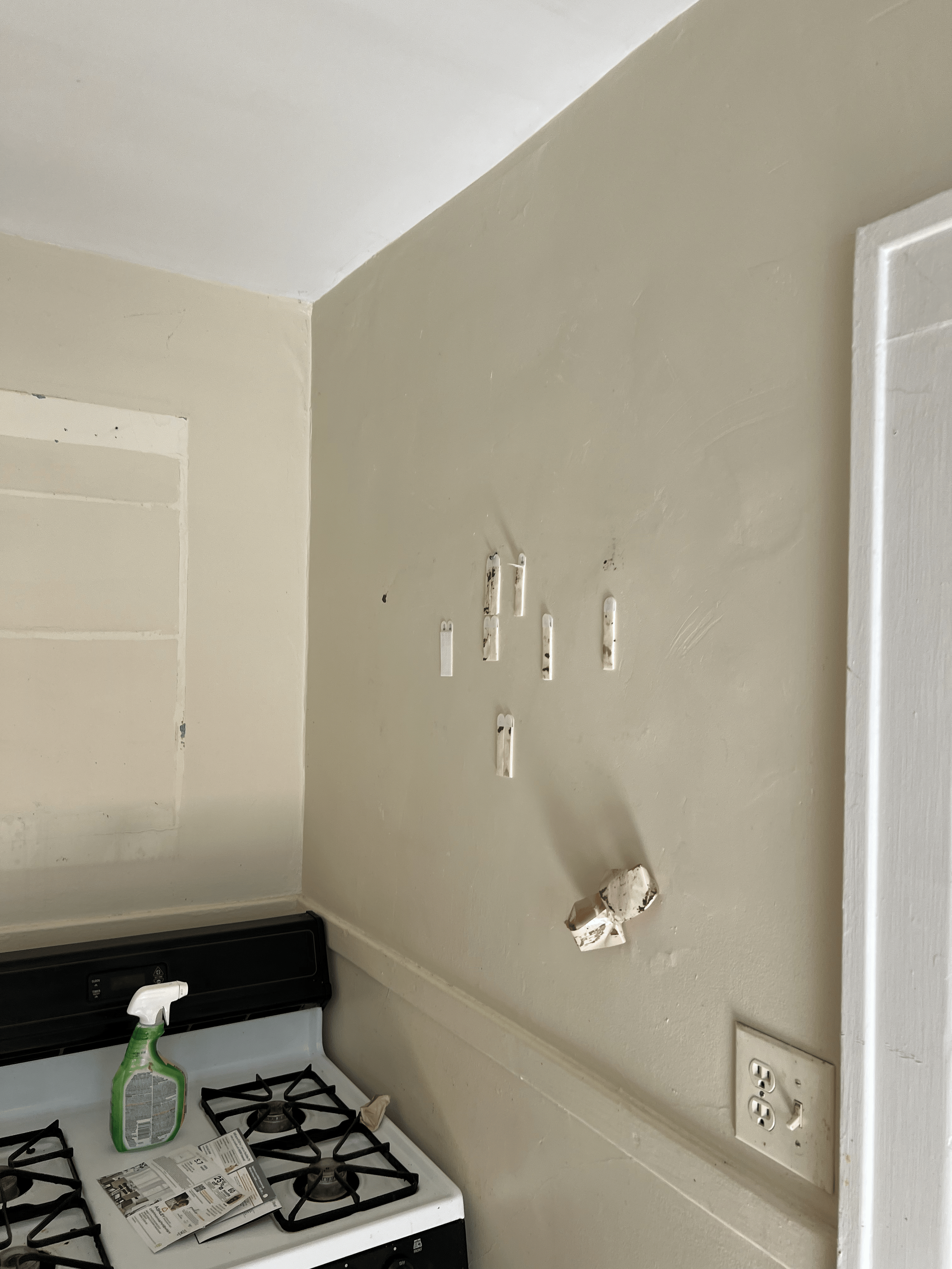
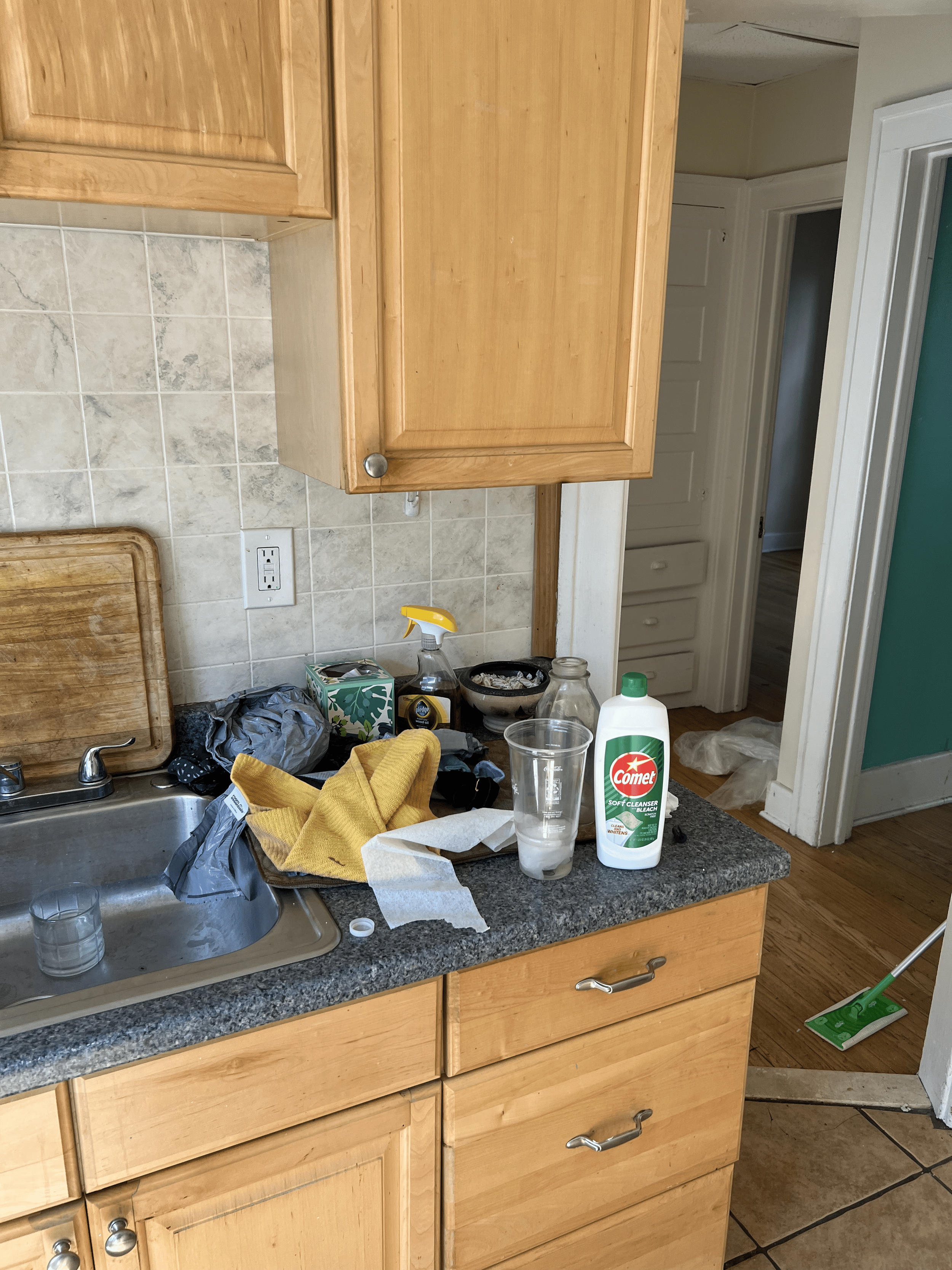
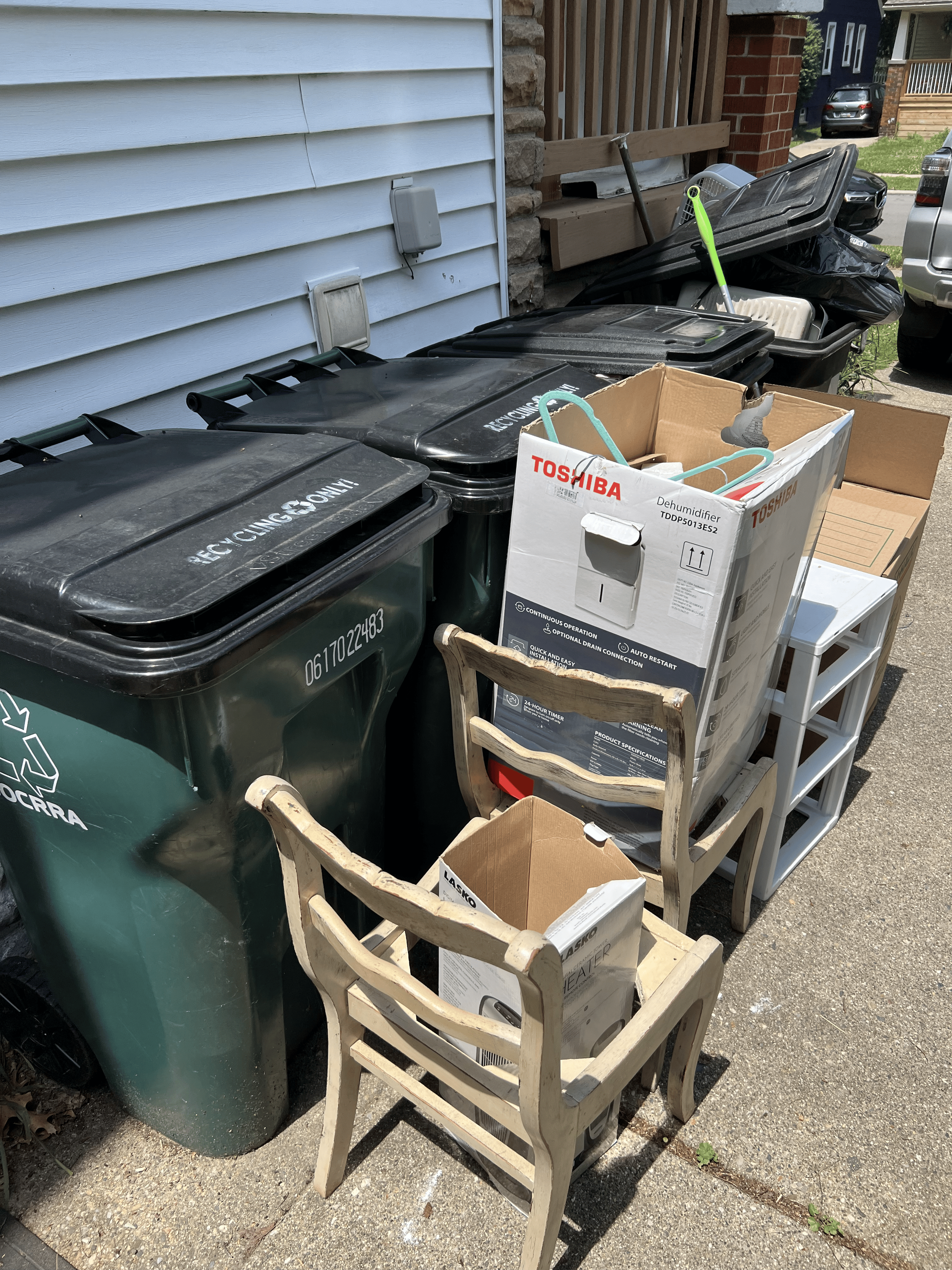
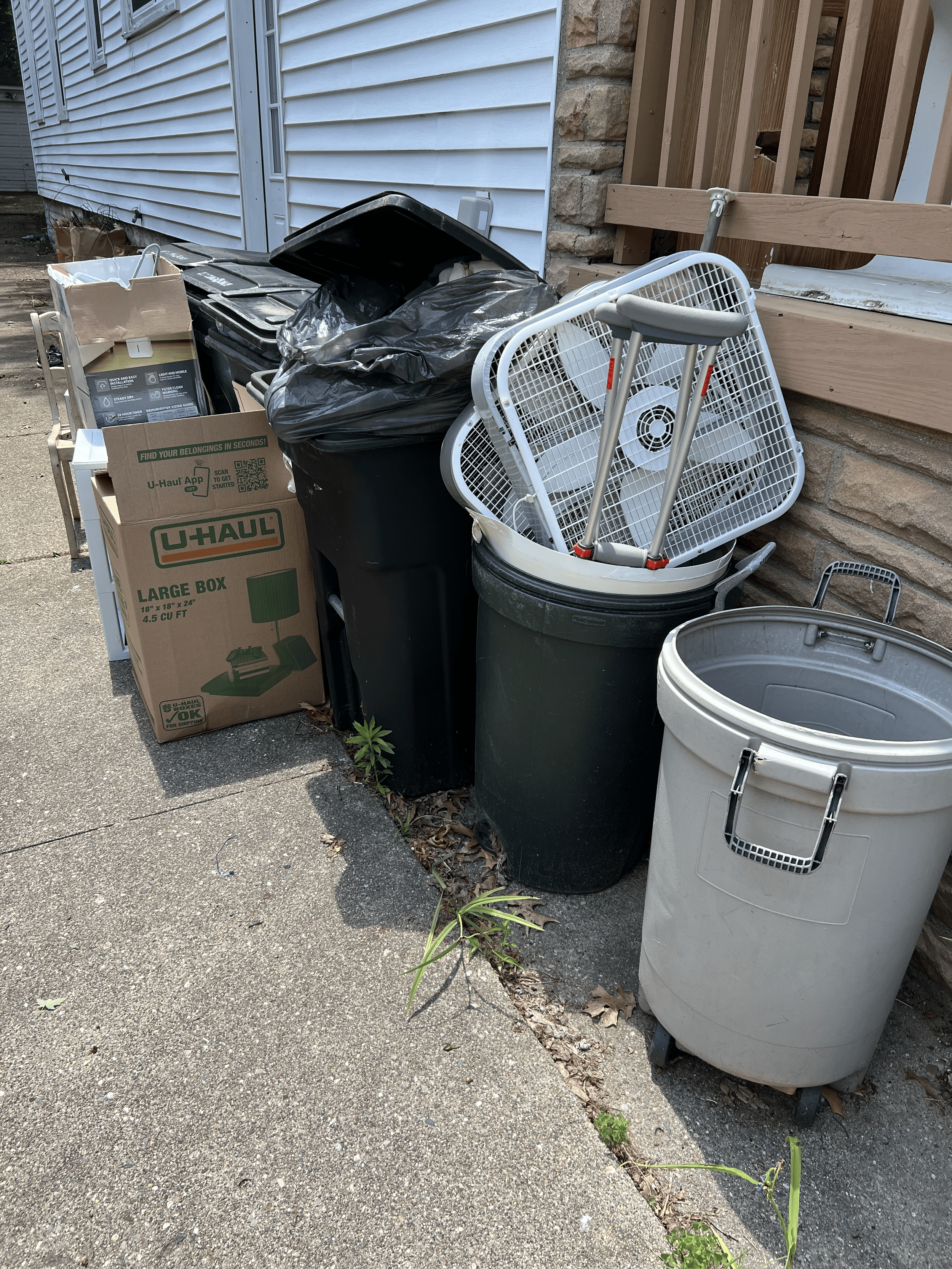
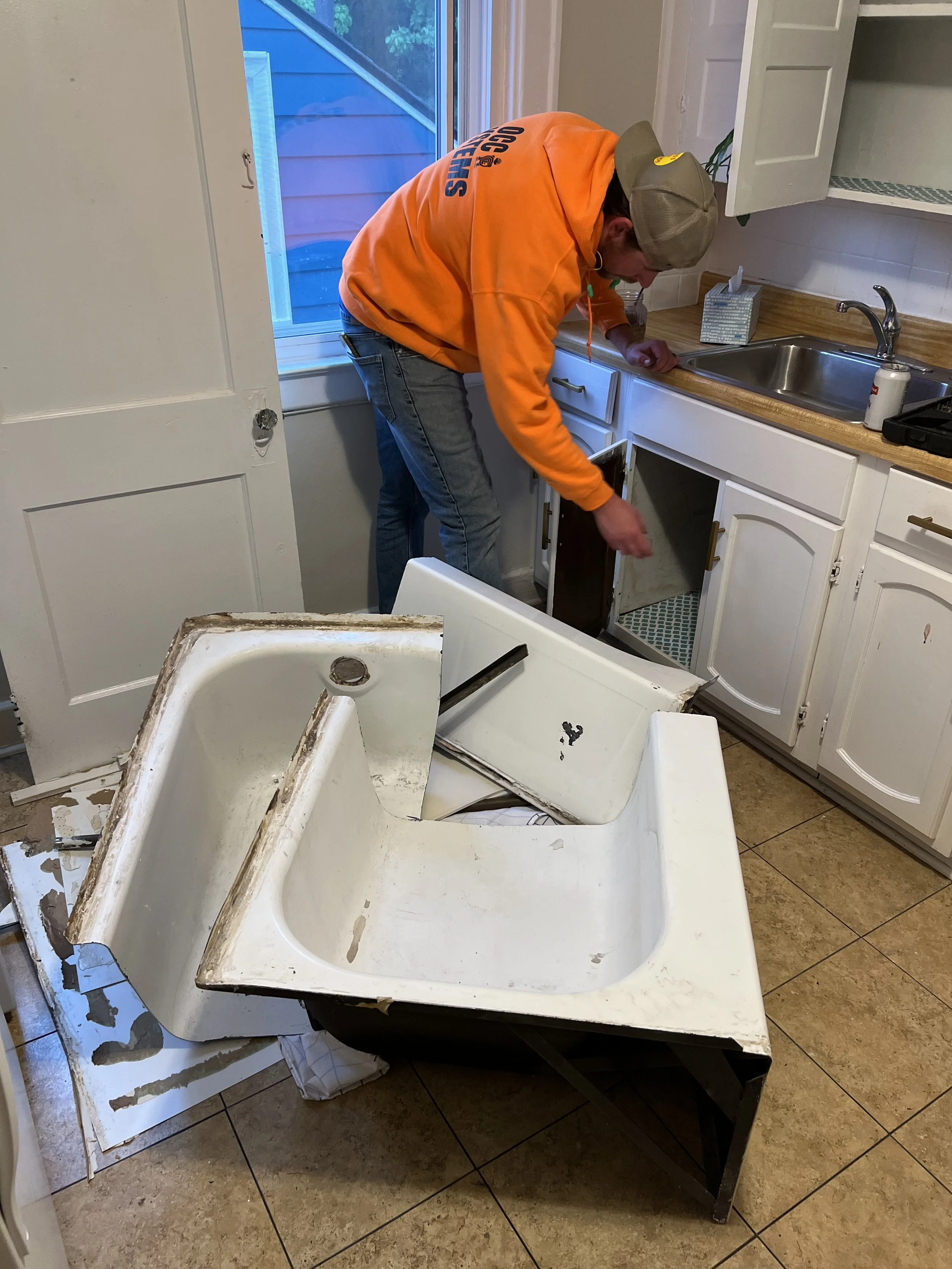
    While functional, the old fridge and oven were in rough shape. The fridge was extremely moldy, missing lots of parts on the interior, and had various juices (including meat) dried all over the front of it. The old oven was incredibly rusty and had grease and grim baked onto it everywhere. In the interest of (current & future) time as well as safety I put both of these appliances on the curb. The 2nd and 3rd images are a before and after of where I removed the old fridge.

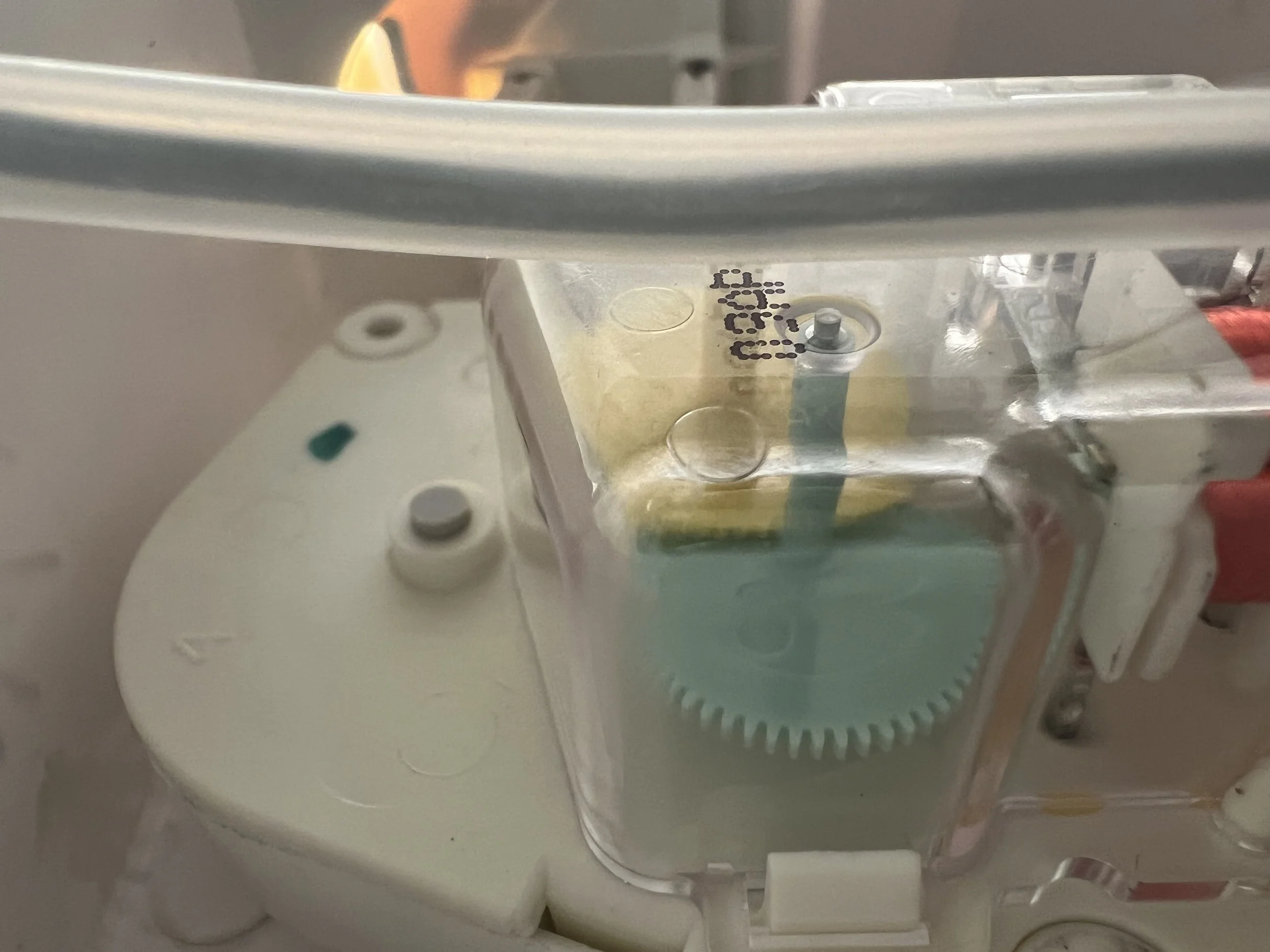
    One day in my unit I notice the fridge was getting warm. I had noticed ice build up in the back of the freezer so I knew that was the issue. I dethawed the whole thing and ordered a new defrost timer. This did not solve the issue, but was a temporary fix until this week (mid Feb 2025). Next I will try the thermal sensor.

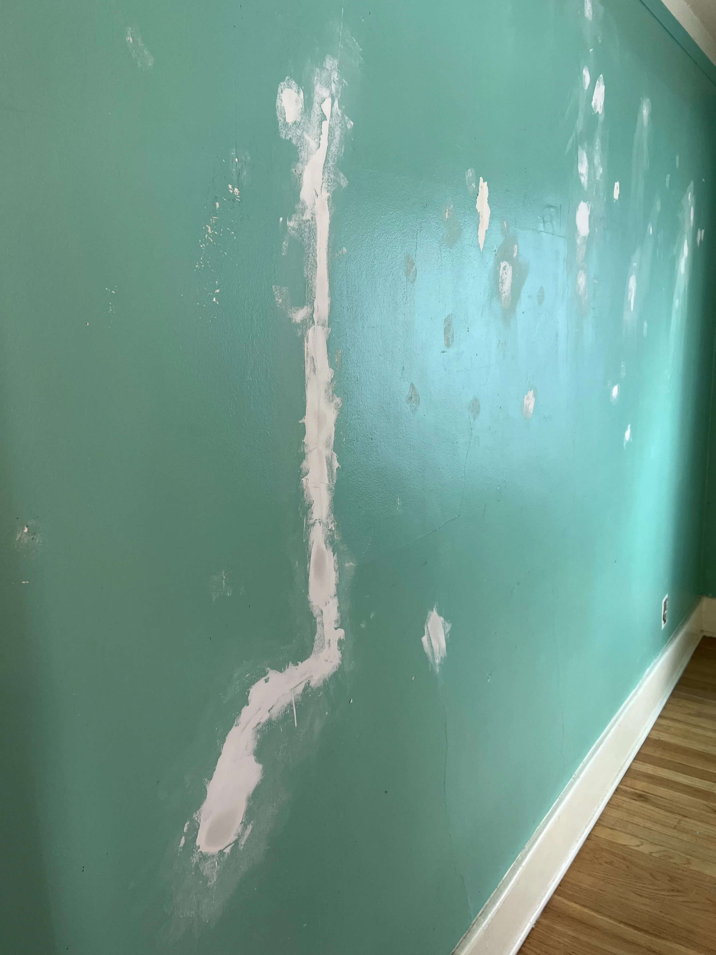
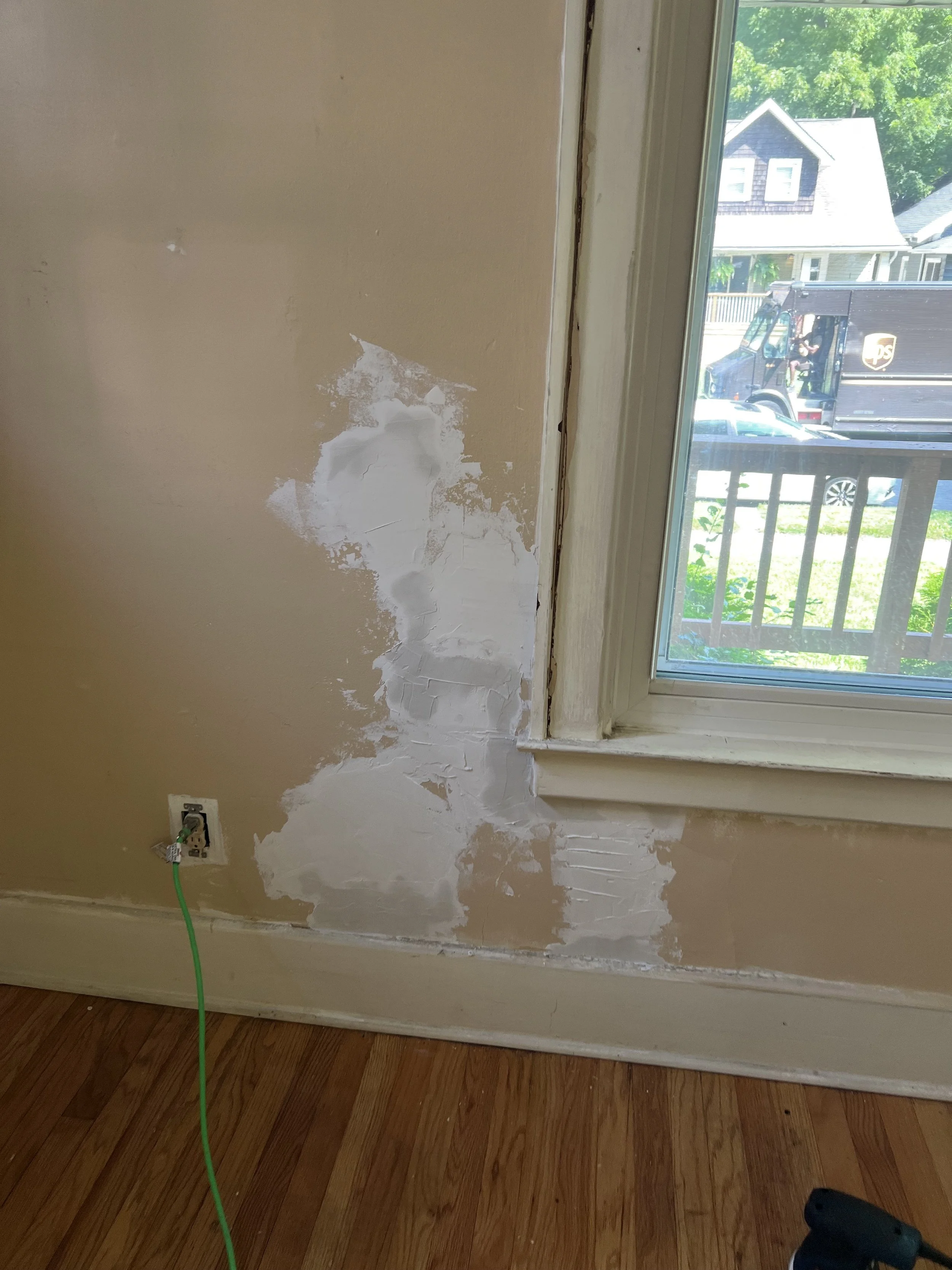
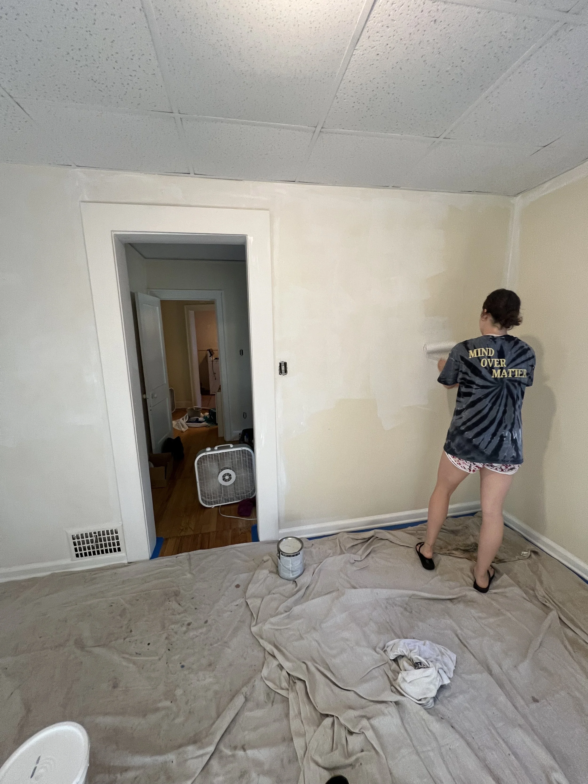
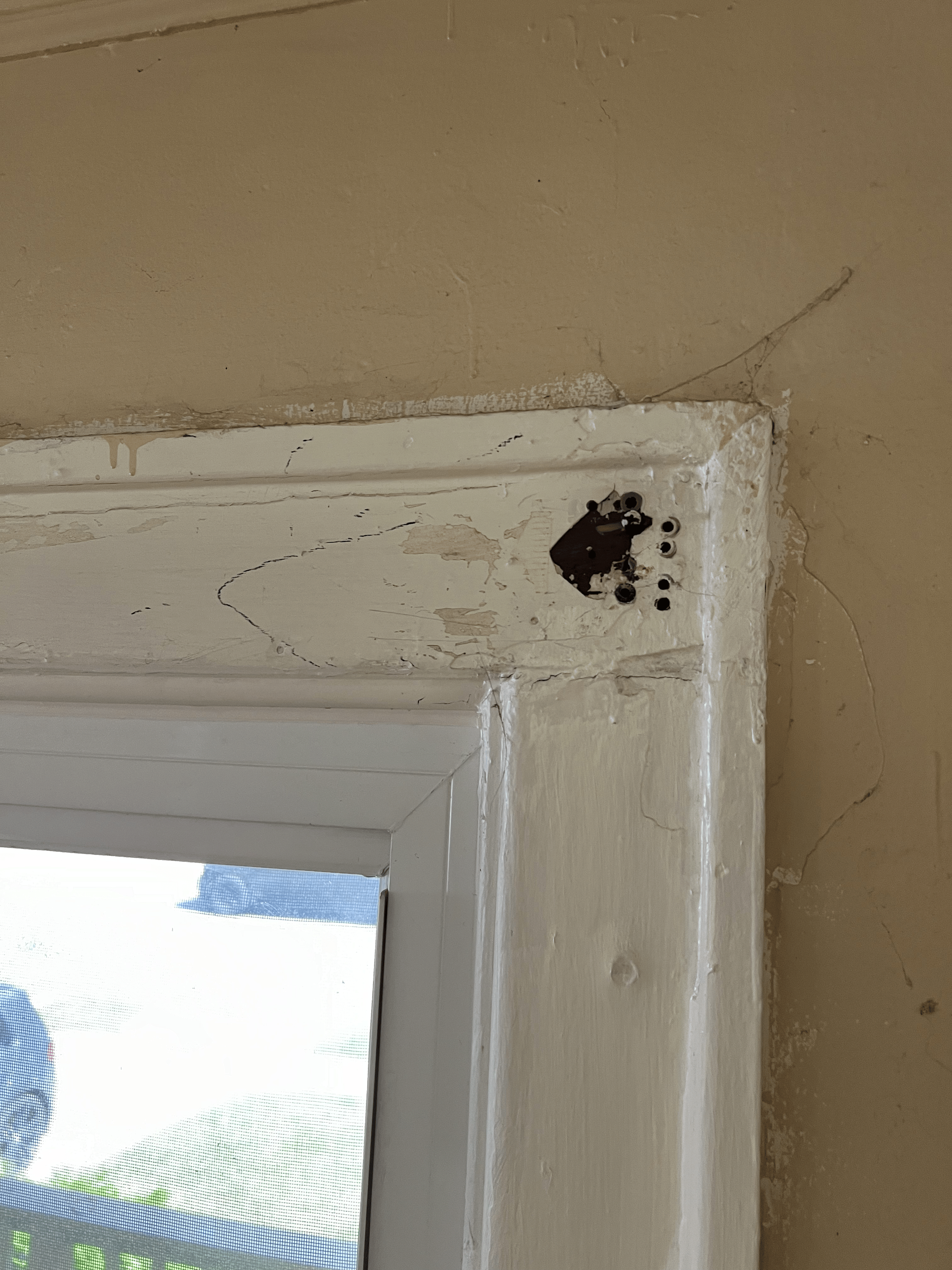
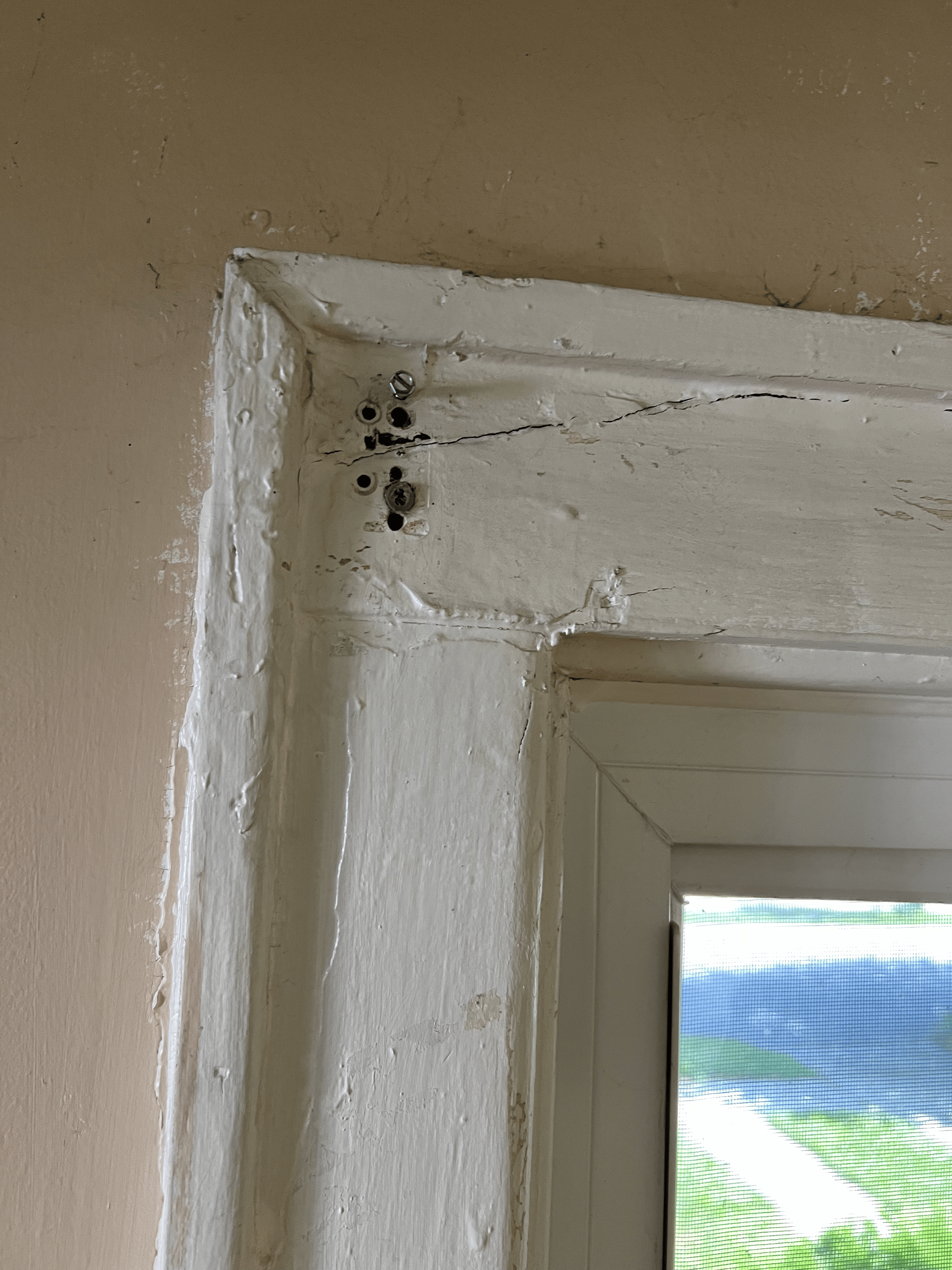
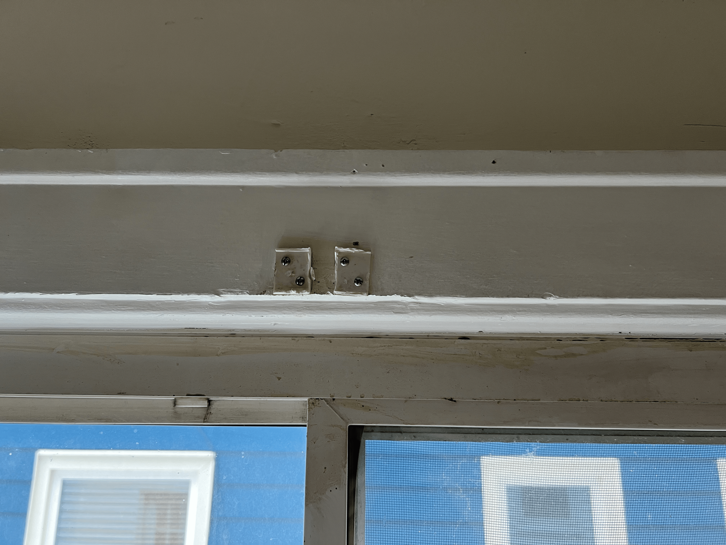
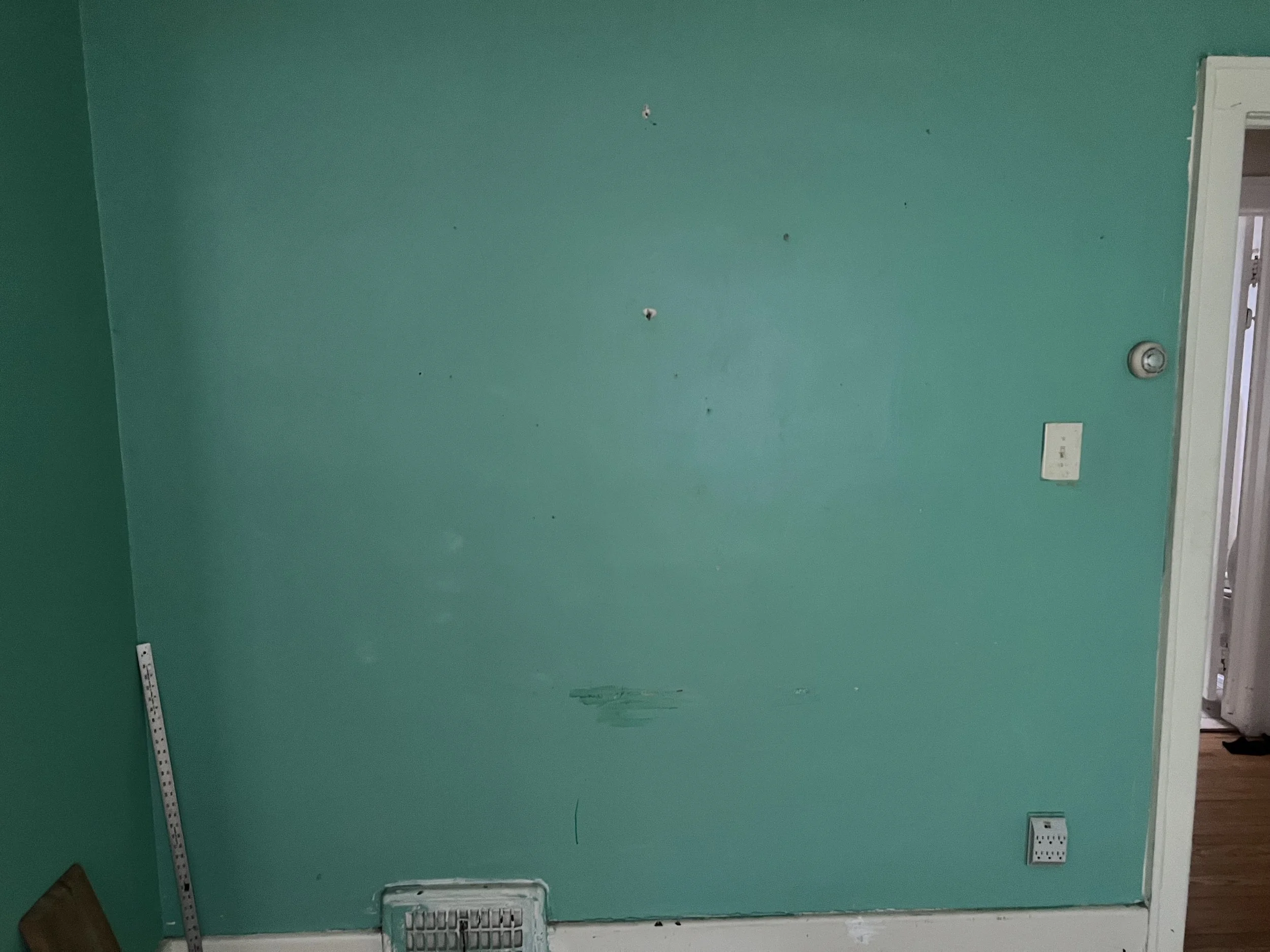
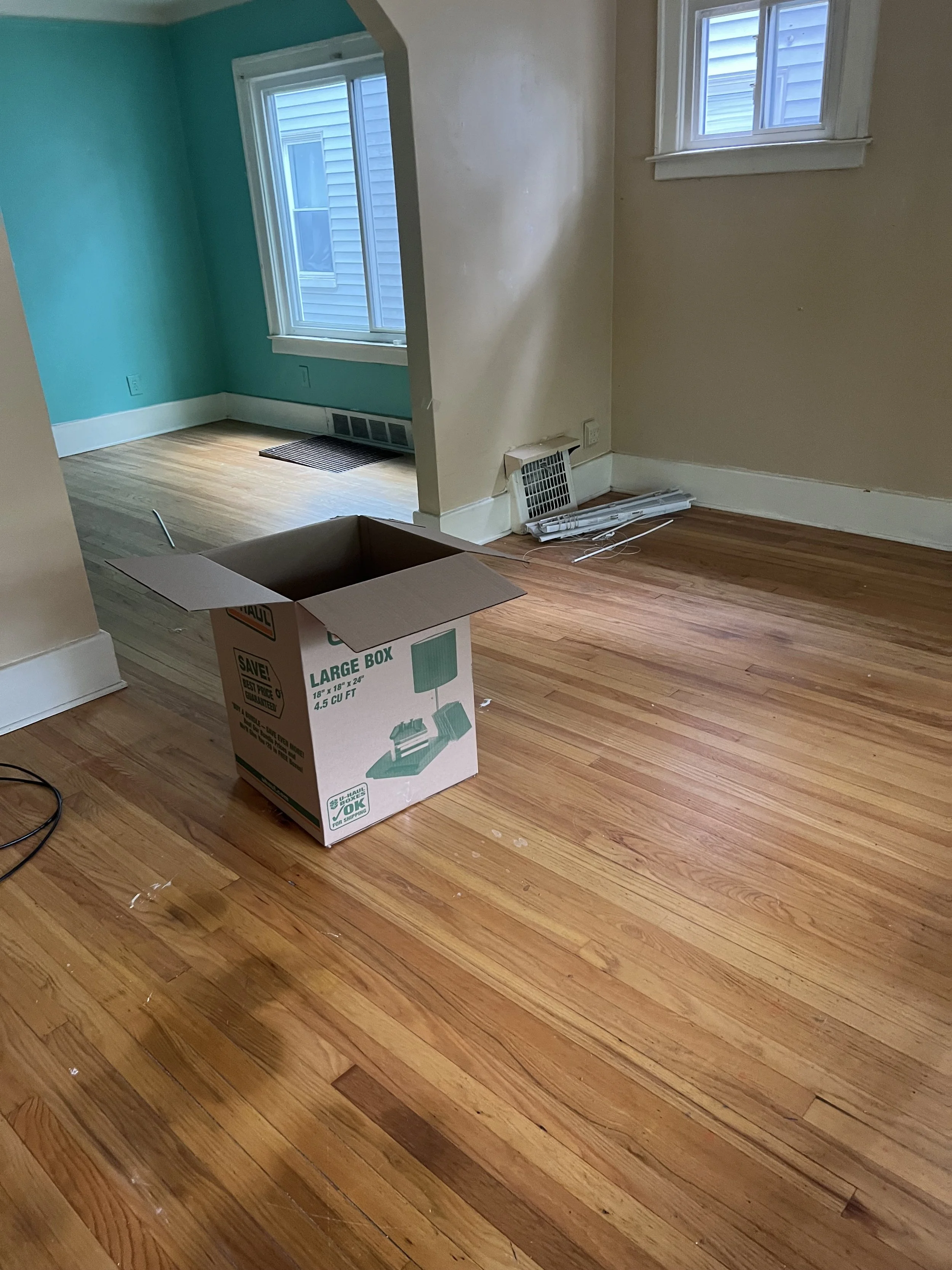
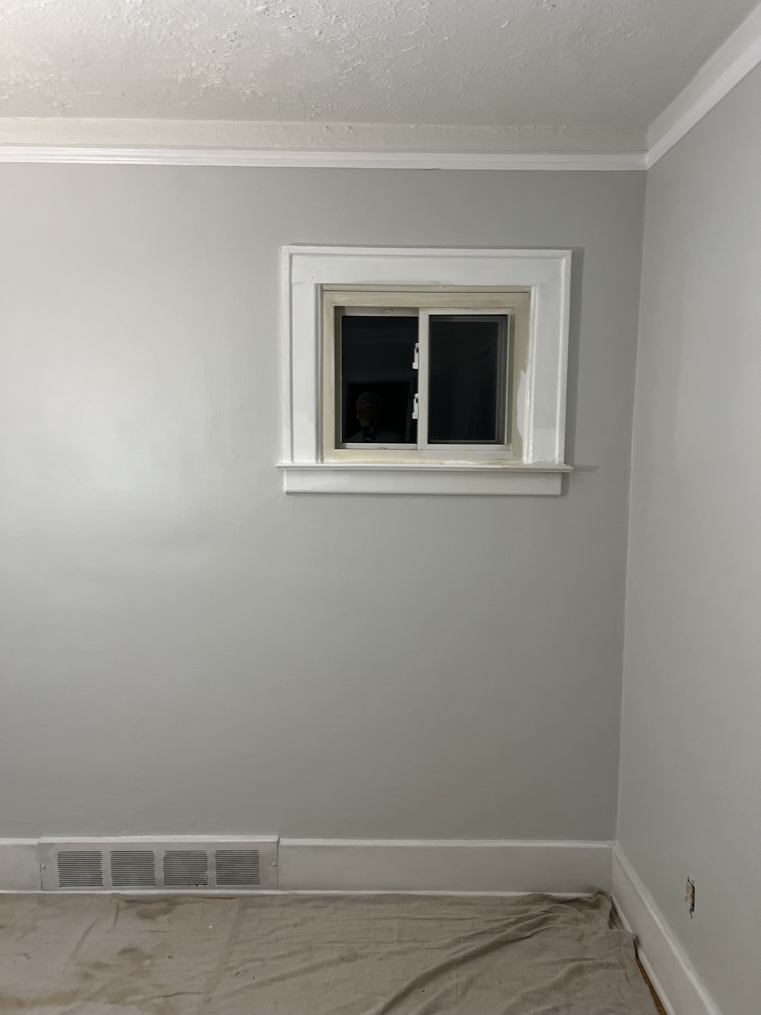
    I ended up painting the living room myself and the image of the window and walls shows the new color I used. I also painted the windows frames and vynl parts of the windows, which you can see the start of in the picture.

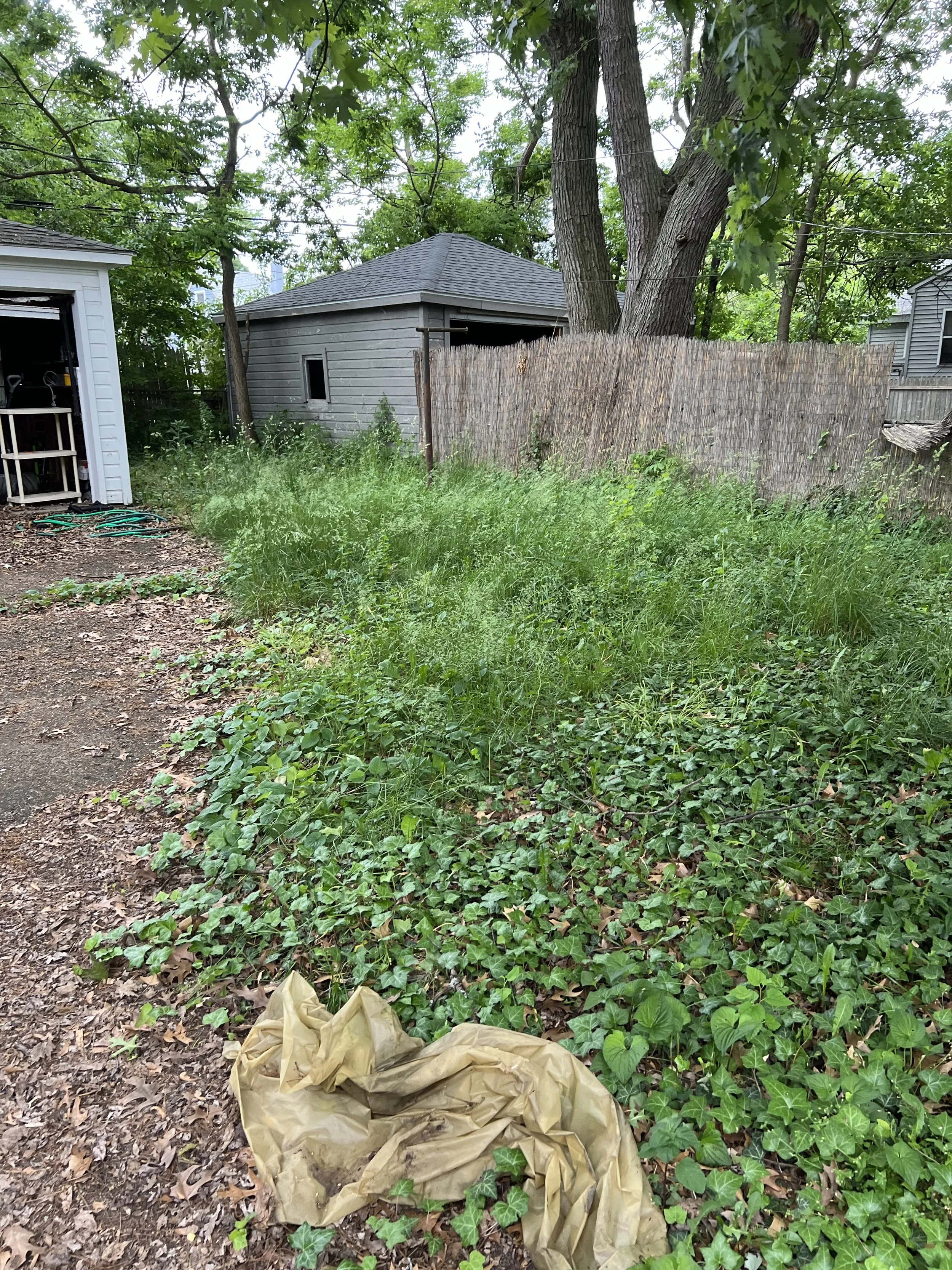
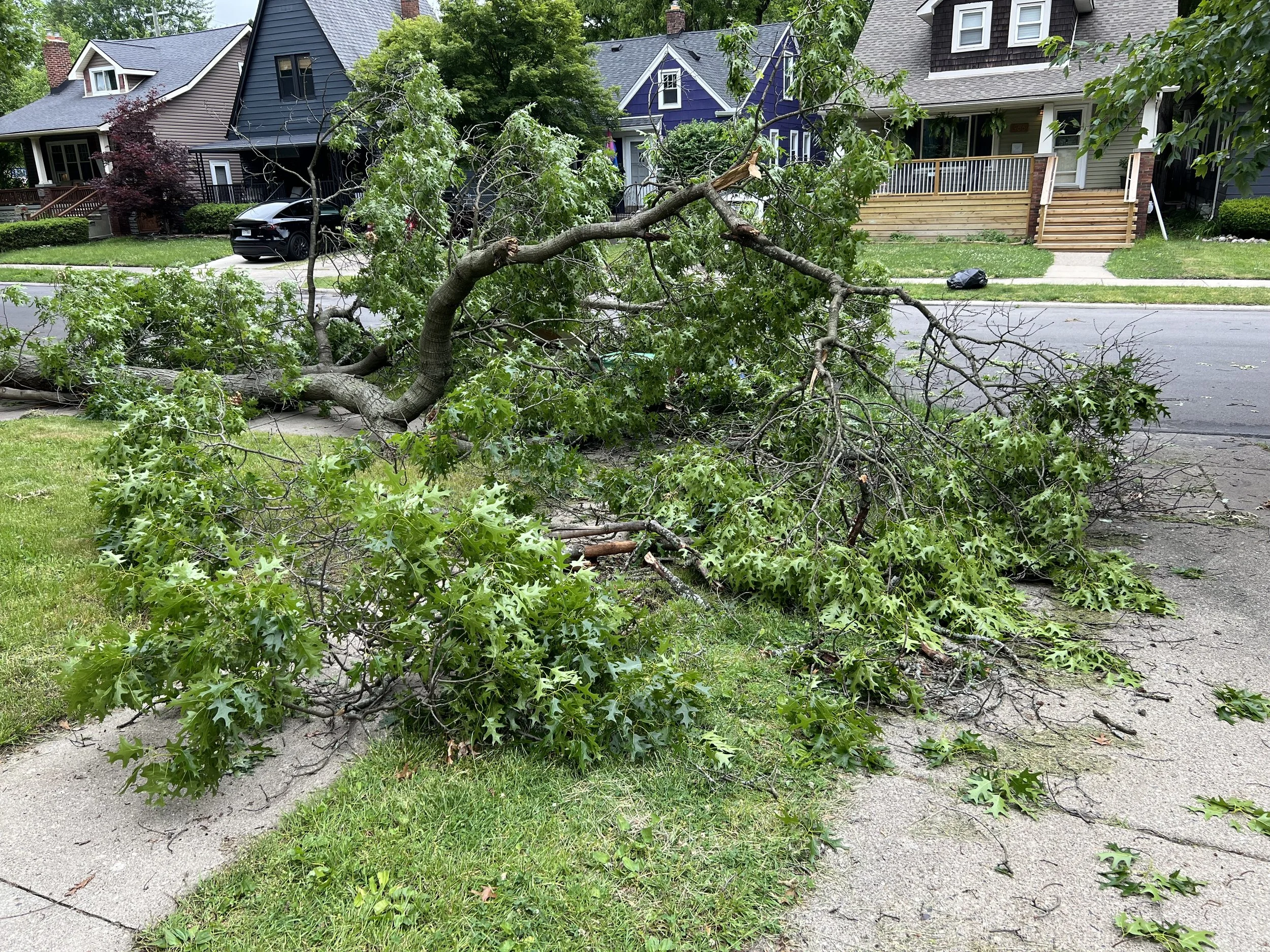
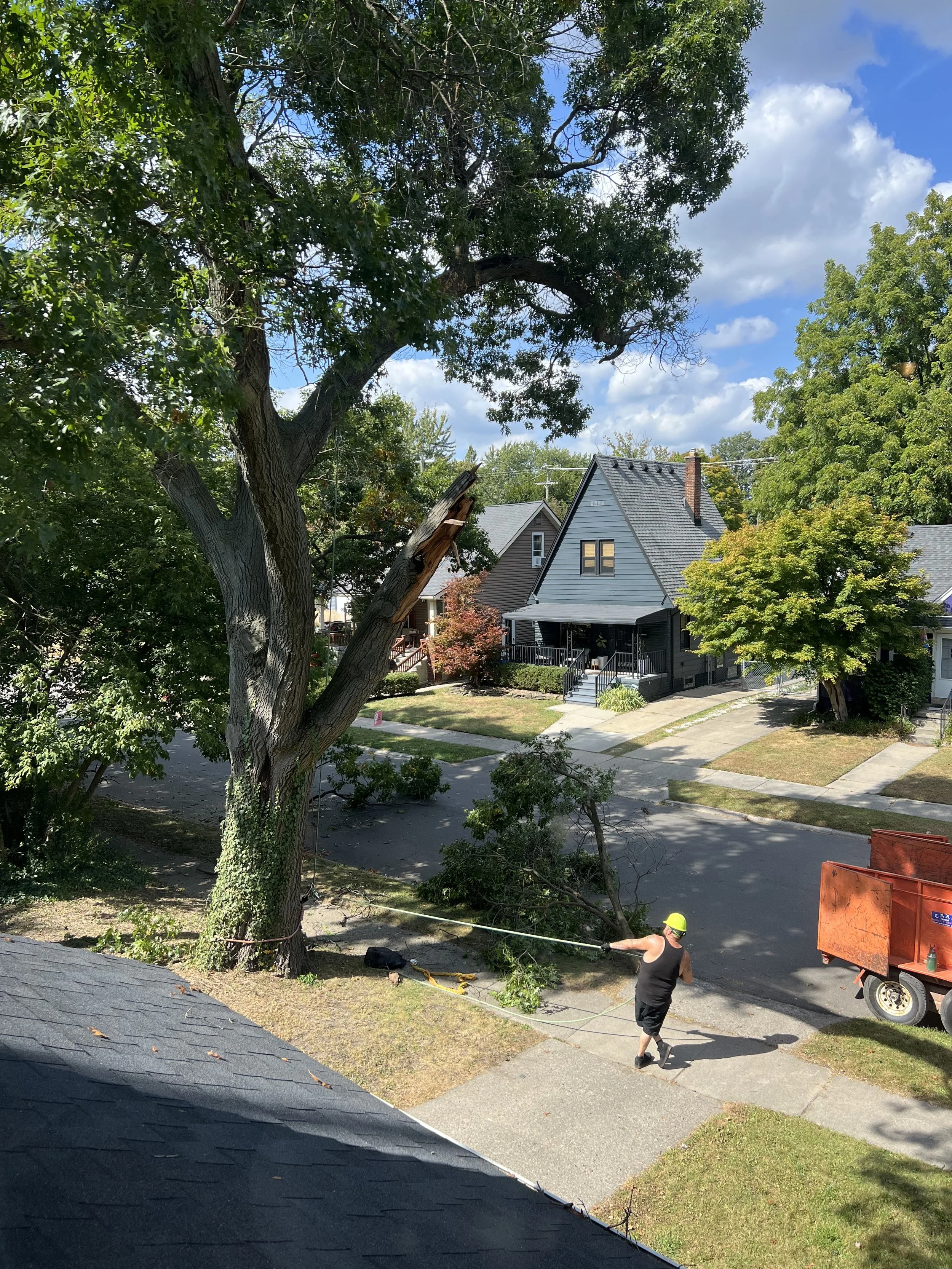
    Dealing with contractors for anything has been a STEEEP learning curve. Finding contractors with integrity and a sense of urgency to get things done in a timely and professional manner has been a huge challenge. I made the mistake of paying a deposit for a tree removal before any work was done. They came a month after I gave them a $1k deposit and cut the branch that least affected me. After several weeks of me nagging and further excuses and delays, I told them not to come back and found someone that finished the job promptly and professionally. I really learned a lot from this. Especially about negotiation, and how important it is to break things down to the basics. The deposit situation taught me to question everything from first principles and push back when something doesn’t add up.

  • Alternator Regulator Study

    Alternator Regulator Study

    Another personal project inspired by electric motors. My friend gave me an alternator he pulled from a mid 2000s GM car in a junk yard (not a subtle jab) here in metro Detroit.

    My vision was to turn this into a wound field electric motor. I planned on designing my own wireless power transfer system and making 3d printed parts to test my design. This is obviously not any type of groundbreaking innovation but rather was meant to be a learning project. It would force me to practice CAD, review power electronics, and test out some control theory. I began by taking apart the brush system and control board, then did DMM testing to make sure the windings were still conductive. I then studied how the control board worked, which was a really good fundamentals of electrical engineering review.

    Shortly after this point I had the idea for my PCB eMotor and pivoted my time towards that project. I believe the PCB eMotor has some truly innovative aspects while incorporating many of the same learnings I would have gotten from this project. Please follow the PCB eMotor project in the dedicated respective posts.

    I will explain my learnings from the control board study below, as there was valuable information in that for me and it became the bulk of my takeaway from looking into alternators.

      Exxotest Guide Used
    Exxotest Guide Used

    The main source of content I used for looking into alternator controls and operation was this guide I found online from Exxotest. Here is the link

    I had to begin with learning about BJT operating principles. There was very little exposure to this in my coursework as most of the focus was on newer switch types. In short, a BJT (Bipolar Junction Transistor) is a semiconductor that controls current flow. When the threshold voltage drop is met across the base and emitter terminals (typically around 0.7V), a small current flows, which modulates the larger current flow between the collector and emitter. This functionality is commonly used as a switch or amplifier and can be doped as an NPN or PNP transistor.

      BJT Symbols
    BJT Symbols

    Conducting State:

    In the conducting state, the rotor is excited and the alternator generates power to charge the battery.

      Conducting Mode Sketch
    Conducting Mode Sketch

    Key aspects of conducting operation:

    • When rotor is excited, transistor T2 is conducting. 

    • The potential across the Zener diode remains below its breakdown threshold, thus preventing the activation of transistor T1 and allowing T2 to conduct. 

    • With T1 open, the base-emitter potential on PNP transistor T2 reaches a sufficient magnitude to initiate conduction.  

    • Though not specified, my assumption is that the base current of T2, and consequently its conduction, is regulated by the ground resistor (Rg). 

    • The voltage divider formed by resistors Ra and Rp establishes the reference voltage applied to the Zener diode. 

    • The output diode acts as a unidirectional conductor, preventing the rotor excitation current from flowing to ground.  

    Non-Conducting State:

    The non-conducting state prevents current flow to the rotor, preventing power generation and battery charging.

      Non-Conducting Mode Sketch
    Non-Conducting Mode Sketch

    Key aspects of non-conducting operation:

    • The fully charged battery voltage provides sufficient potential to overcome both T1’s Vbe drop and the Zener breakdown voltage, facilitating base current flow through the Zener diode. 

    • When T1 saturates, its low collector-emitter voltage (Vce) reduces the base-emitter voltage (Vbe) of T2 below its activation threshold. This is because a saturated BJT exhibits a very low Vce, typically 0.1V to 0.2V, which is less than the typical 0.7 Vbe activation threshold. 

    • With T1 active, current diverts to ground via the ground resistor (Rg). 

    • This design opens T2 while minimizing T1 current draw, preventing rotor excitation in a high-charge state. 

    LT Spice Simulations:

      Diode Rectification Circuit
    Diode Rectification Circuit
      Diode Rectification Circuit - Voltage Plot
    Diode Rectification Circuit – Voltage Plot

    I am very much a visual learner. I created this LT Spice model so that I could visualize the inputs and outputs as well as exploratory analysis of circuit behavior. I believe the voltage drop between the output and input waveforms is due to the diode. If you take a look at the difference between the cursors, the maximum difference is about 0.9V. This is close to 0.7V, which is typical for a PN junction. The low-value resistor creates a high load, which likely influences the diode’s voltage drop and output voltage ripple. I tried adding a 1mF capacitor across the output and this removed all of the ripple in the output voltage.

      Zener Diode Test Circuit
    Zener Diode Test Circuit
      Zener Diode Test Circuit - Voltage Plot
    Zener Diode Test Circuit – Voltage Plot

    I also created this circuit for visualization purposes. The breakdown voltage of this particular Zener diode is 8.2V. You can see that the voltage rolls off at this point and flattens out as current begins to flow through the reverse biased diode.

    Conclusions:

    This project served as an effective review of circuit fundamentals and offered a practical opportunity to study BJT switches. It was really neat to see an example of a control strategy using only analog components. In the future, I’m interested in looking into the complexities of the Rp resistor in the voltage divider circuit.

  • August 2024 – Priming & Painting

    August kicked off with a huge help from my wonderful family! They tackled the priming of the bottom unit, while I dove headfirst into the walls. Ten layers of cracking paint clinging to cracking lath and plaster presented a serious challenge. My tools and materials included joint compound, wood glue, an orbital sander, and foam sanding blocks. It was a meticulous process, but the results were worth it.

    The living room ceiling, also lath and plaster, was in even worse shape, riddled with cracks and sagging from years of Midwest humidity seeping in through open windows. Plaster washers, liquid nails, and more wood glue became my go-to solution. After securing the plaster, I applied a fresh layer of drywall mud, carefully matching the existing ceiling texture for a uniform appearance.

    A few weeks later, my amazing girlfriend (now wife!) helped transform the rooms with fresh coats of paint, breathing new life into the space. I continued the wall repairs, painted all the laith and plaster ceiling, meticulously painted the trim and window frames, and replaced outdated outlets throughout the house. The “vanilla bean” (aka “cigarette yellow,” my friend’s spot-on description) and the disgusting turquoise dining room are finally gone (objective opinions).

    I wish I had more photos to share from this period, but unfortunately, I was more focused on getting things done and hadn’t considered needing the pictures for anything later.

  • June/July 2024 – Paint Prep

    Summer 2024 presented a complex project management challenge: balancing eight weddings (only 3 in state), a 10-day work trip to Cologne in June, and the ongoing house renovation. During the little time I had in June and July, the focus was on preparing the lower unit for painting, addressing inherited tenant issues (including legal and police involvement), and moving myself into the upper unit. In the midst of the whirlwind, documenting the renovation was not a priority. These few photos offer a small window into the work that was done during these months.

  • May 2024 – Getting Started

    I closed on the property in the spring, but the renters’ occupancy pushed my access back to the end of May and early June. The state they left the property in dictated my first steps: a major trash clean-out, serious yard work, and essential maintenance. Once those were complete, I turned my attention to a bathroom demolition upstairs.

    The upper unit bathroom was ground zero for the renovation. The previous tenant moved out before the bottom one and left the place picked up. In general, this space had clearly been neglected (by landlords mainly) for at least a decade (and in some areas, much longer). The “handyman” work was rough, including this shower situation. Installed with the incorrect adhesive, it was leaking and practically peeled off the wall. At first, I thought the tub was cast iron and tried the sledgehammer method… Nope, steel. The hammer just bounced back and left a dent when I hit the tub harder. Thankfully, my friend came to the rescue with his sawzall and some carbide blades. Cutting it out was surprisingly easy. Then came the floor. Two layers of linoleum/vinyl over particle board screwed into the original oak floor (tears). As you can see, the leaky tub had done its damage, turning the subfloor into a moldy disintegrating mess.

    Figuring out the original 1922 layout of this house is like solving a historical mystery, the wall behind the shower framing is a major piece of the puzzle.

    The photos above highlight the yard work and trash that were kindly left behind for me to deal with. Around the time I gained access to the property, one of two oak branches cracked and fell. The one that fell was thankfully over the yard. Its twin is over the front half of my house. More on that in a later post…

  • Cu vs. Al Resistance Considering Skin Effect

    Cu vs. Al Resistance Considering Skin Effect

    This short research topic came up through discussion with my coworkers. We all knew that copper had lower resistance than aluminum and that it was due to resistivity, but didn’t know the details of that. We realized that none of us could answer the question “Why does copper have a smaller skin depth than Aluminum?” To gain a complete understanding, we naturally turned to first-principles physics. 


    The DC Case: 

    Copper has a lower intrinsic resistivity than aluminum, which is a multiplier in the formula for resistance: 

    R = ρ * (L / A) where: 

    • R is resistance (Ohms) 

    • ρ is resistivity (Ohm-meters) 

    • L is length (meters) 

    • A is cross-sectional area (square meters) 

    Lower resistivity means the material is a better conductor.  

    When an electric field is applied across a conductive material, it causes electrons to move in a specific direction relative to the field. Electrons of equal magnitude are the charge carrier in both copper and aluminum.  


    Consider the equation for approximating conductivity (Drude Model), which is the inverse of resistivity: 

    σ ≈ (n * q² * τ) / m   (m is the effective mass of the electron)  

    τ is the mean free time, which is longer in copper due to its atomic structure resulting in less scattering of electrons compared to aluminum. 


    Understandably, electron mobility is the main factor in the resistivity of materials. Copper’s electrons have the ability to move more freely, leading to higher conductivity or inversely lower resistivity.  

    Room Temperature Resistivity values:  

    Copper: ≈ 1.68 x 10⁻⁸ Ohm-meters 

    Aluminum: ≈ 2.65 x 10⁻⁸ Ohm-meters 

    Aluminum is roughly 1.58 times more resistive than copper.  

    The AC Case (skin effect):  

    Let’s look at the equation for skin depth: 

     δ = 1 / √(π * f * μ * σ) Where: 

    • δ = skin depth (meters) 

    • f = frequency  

    • μ = magnetic permeability ≈ μ₀ = 4π x 10⁻⁷ H/m (for both copper and aluminum) 

    • σ = electrical conductivity (S/m) 

    As described in the DC section, copper has a higher conductivity than aluminum. Looking at the formula above we can see that larger conductivity value will result in lower skin depth. As a result, the skin depth of copper at any given frequency is going to be less than aluminum.  

    The question remains, “what causes skin effect?”  

    With AC current, the direction and magnitude of the flow of electrons is constantly changing. Due to Ampere’s law, the changing current creates a fluctuating magnetic field around the conductor. This changing magnetic field induces a voltage within the conductor (Faraday’s Law), which in turn drives eddy currents. Lenz’s law dictates that the induced eddy currents always oppose the change in magnetic field. The changing magnetic field is strongest in the center of the conductor. Consequently, the eddy currents in the center flow opposite to the main current, which create an opposing magnetic field that pushes the main current away to the edges of the conductor. This situation can be thought of as the center of the conductor having an inductive impedance. Current wants to flow in the path of least resistance, therefor redistributing to the surface of the conductor.  

    Summary:

    What we really wanted was to understand why skin effect happens. Working through the cause-and-effect using Maxwell’s equations helped us get there and provided the understanding we were looking for. It’s now clear that the skin effect is the direct reason for power losses in conductors at high frequencies – those “AC losses” that are so important to consider when designing electromagnetic systems.

    Materials Used:

  • LiDAR Learning

    LiDAR Learning

    LiDAR learning was my senior design project in my final semester at Purdue. I worked as an electrical engineer on a team of 4 with three computer engineering students. My responsibilities were to guide and lead the team as well as develop the power system for the project and design the PCB for our end product.

    Please see below for more details on the project!

      Project Photo
    Project Photo

    Project Overview

    The primary goal of this project is to design a device that assists teachers in identifying potential threats outside their classrooms without compromising their safety. The device integrates a camera mounted on a servo motor, a LiDAR sensor, and a light sensor to provide a comprehensive monitoring system. The camera captures real-time video, while the LiDAR sensor detects the location of subjects outside the classroom. This data is processed by a microcontroller, which controls the servo motor to keep the subject centered on the monitor inside the classroom. Additionally, an LED light is activated in low-light conditions to ensure clear visibility.

    Demo Video

    Inspiration

    The Oxford High School shooting during my Fall 2021 internship in Michigan took place nearby and deeply affected me. As an engineer, I immediately began thinking about how technology could help mitigate such tragedies. My initial concept involved a comprehensive defense system using strategically placed LiDAR sensors throughout a school to track individuals in real-time. This LiDAR tracking data would be the input for a neural network designed to identify potential threats and, based on its analysis, control the building’s doors. By analyzing movement patterns, the system could identify potential threats and quickly and safely contain them, limiting their mobility. This would allow students and staff in unaffected areas to evacuate safely while the threat was isolated.

    Budget Constraints

    Due to a limited budget of approximately $400, the project scope had to be significantly reduced. This constraint prevented the team from developing the multiple-device system and incorporating the machine learning capabilities of multiple scanners that my original vision entailed. Despite these limitations, we successfully created a functional safety device using a single 2D LiDAR scanner and a camera.

    Key Features and Design Requirements

    1. LiDAR Sensor: The RPLiDAR sensor scans the hallway and detects moving subjects. It provides accurate distance and angle measurements, which are used to control the camera’s movement.

    2. Camera and Servo Motor: The camera pedestal rotates to follow the moving subject as indicated by the LiDAR mapping. This ensures continuous monitoring of potential threats.

    3. Light Sensor and LED: A photoresistor detects the brightness of the environment and activates an LED fixture if the hallway is too dark. This feature ensures that the camera can capture clear video even in low-light conditions.

    4. Power Supply: The device is powered by a standard wall outlet, making it easy to install and use in any classroom.

    5. User-Friendly Interface: A TFT display inside the classroom receives continuous live video feed via WiFi connection. An on/off switch is located next to the display for easy control.

    System Integration and Operation

    The system is designed for easy mounting outside classrooms and is powered by standard wall power. The LiDAR sensor continuously scans the surrounding area, tracking the closest object and rotating the camera to the corresponding angle. During a lockdown, the integrated illumination system activates, ensuring clear visibility for the camera. The video feed is then wirelessly transmitted to a display inside the classroom, allowing teachers to monitor the situation without exposing themselves to potential threats.

      System Block Diagram
    System Block Diagram

    System Block Diagram Explained

    The 5 Subsystems

    • RPLiDAR – Self-contained LiDAR, controlled by ESP32-S2

    • ESP32-S2 – Main controller, processes LiDAR data, controls hardware

    • ESP32 – Camera/controller interface, Bluetooth communication

    • Camera Support – Servo-driven camera mount, light sensor, lighting

    • Power System – AC/DC converter, 3.3V buck converter

    My Responsibilities:

    As the EE guy on the team, my main responsibility was to design the power system for the project. The +3.3V rail powers the ESP32-S2 and its USB interface components, while the +5V rail powers the remaining components and sensors. The external display is powered via a dedicated +5V DC cable.

      Power Subsystem Block Diagram
    Power Subsystem Block Diagram

    Buck Converter

    I designed a buck converter voltage regulator using TI’s LMZ10504. Prototyping on a copper clad board proved challenging. After resoldering two times, I was confident it wasn’t a soldering issue or design flaw. Throughout the process, I used an oscilloscope to verify inputs and outputs and double-checked my feedback loop design. Despite the resistors being within the datasheet’s specified range, my testing pointed to the feedback loop as the problem.

    Confused, I consulted our lab mentor, a retired circuit designer with over 40 years of experience. He independently diagnosed the issue as the feedback resistors, specifically R1 and R2. While the datasheet values seemed appropriate, they were too high, preventing sufficient current from reaching the IC’s feedback pin for proper regulation. We lowered the resistor values, and the regulator then functioned as expected. This taught me a valuable lesson of the importance of experience; sometimes, theory and datasheets just aren’t enough.

    PCB Design

    During one of my internships, I gained experience reading schematics and PCB layouts, and sat in on a design review where experienced avionics designers critiqued a junior designer’s work. Those two hours were a crash course in PCB design.

    For our senior design project, I volunteered to design the PCB, which involved consolidating subsystem schematics and tackling the puzzle of component placement. Our focus was on placing components according to physical interface locations, not size or efficiency. While I wouldn’t want to do it 100% of the time, I find PCB design, like coding, to be a rewarding exercise.

    Whether through luck or thorough preparation, our PCB and components worked perfectly after assembly. Teammates 3D-printed camera and controller enclosures, and we had a laser-cut enclosure fabricated. We were quite happy and proud of how our final product turned out!